Preparation method of metal-oxide-semiconductor field-effect transistor with silicon-on-nothing (SON) structure

A gate region and active region technology, which is applied in the field effect transistor manufacturing process and the MOSFET manufacturing process field, can solve the problems of complex process, affecting yield and high cost, and achieve simple process, production cost saving, and yield improvement. Effect

Inactive Publication Date: 2012-02-01
SHANGHAI INST OF MICROSYSTEM & INFORMATION TECH CHINESE ACAD OF SCI
View PDF7 Cites 8 Cited by
  • Summary
  • Abstract
  • Description
  • Claims
  • Application Information

AI Technical Summary

Problems solved by technology

This method is complex in process, high in cost, difficult to control the quality of the source and drain regions and affects the yield

Method used


Image

  • Preparation method of metal-oxide-semiconductor field-effect transistor with silicon-on-nothing (SON) structure
  • Preparation method of metal-oxide-semiconductor field-effect transistor with silicon-on-nothing (SON) structure
  • Preparation method of metal-oxide-semiconductor field-effect transistor with silicon-on-nothing (SON) structure

Examples


Embodiment Construction

[0017] The device structure of the present invention will be further described below in conjunction with the accompanying drawings, which are not drawn to scale for the convenience of illustration.

[0018] Please see Figure 1-4 , using the preparation method of the present invention, taking a CMOS device as an example, comprises the following steps:

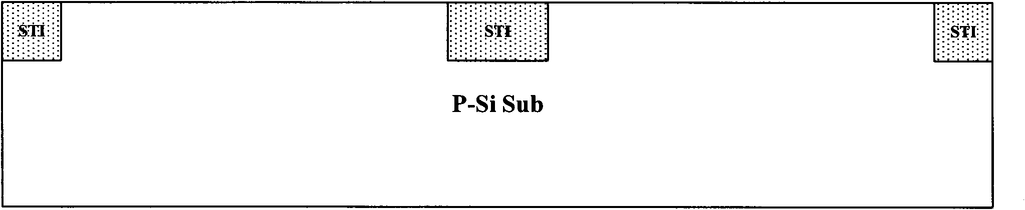
[0019] Step 1, such as figure 1 As shown, the active region is formed on the bulk silicon substrate (p-type Si substrate) by shallow trench isolation technology, which is exactly the same as the traditional bulk silicon CMOS process.

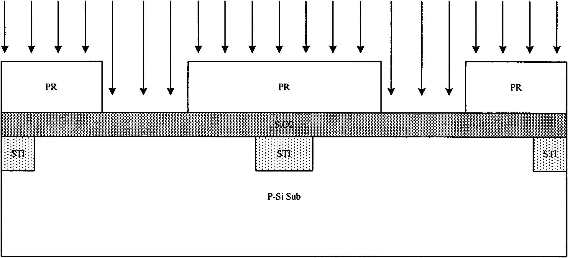
[0020] Step 2, forming a layer with a thickness on the active region by thermal growth or LPCVD Above SiO 2 The buffer layer.

[0021] Step three, such as figure 2 As shown, using a photolithography plate for the gate region, the photoresist with the opposite polarity to the photoresist used in the photolithography process for the gate region is used for photolithography, so that the posit...


PUM


Abstract

The invention relates to a preparation method of a metal-oxide-semiconductor field-effect transistor (MOSFET) with a silicon-on-nothing (SON) structure, which is characterized in that: a buffering layer is grown on a silicon underlay, then a gate-region photolithography mask is utilized to be photoetched through photosensitive resist with a polarity being opposite to that of photosensitive resist for gate-region photoetching technique, so a position for forming the gate region on an active area is exposed, then hydrogen ion and helium ion are injected, and a hollow layer is formed inside the active area below the position of the gate region through annealing after removing the photosensitive resist; and finally the buffering layer is removed, and the standard complementary metal-oxide semiconductor (CMOS) technique is carried out. Due to the adoption of the method, the MOSFET having the SON structure only with an MOS channel having a hollow layer is realized, and the process of the source-drain region is not influenced; and the gate-region photolithography mask of the standard CMOS technique is used for defining a hydrogen and helium injection window, so an additional photolithography mask is unnecessary to prepare, and the automatic aligning of the hollow layer and the gate-region position can be realized.

Description

technical field [0001] The invention relates to a manufacturing process of a field effect transistor (MOSFET), in particular to a manufacturing process of a MOSFET with a SON (Silicon On Nothing) structure, and belongs to the technical field of semiconductor manufacturing. Background technique [0002] SOI (Silicon On Insulator) refers to silicon-on-insulator technology. Because SOI technology reduces the parasitic capacitance of source and drain, the speed of SOI circuit is significantly improved compared with the speed of traditional bulk silicon circuit. At the same time, SOI also has a small short-channel effect. , good anti-lockup, simple process and a series of advantages, so SOI technology has gradually become the mainstream technology for manufacturing ultra-large-scale silicon integrated circuits with high speed, low power consumption, high integration and high reliability. However, SOI devices have a self-heating effect, which will lead to degradation of device per...

Claims


Application Information

Patent Timeline
Patent Type & Authority Applications(China)
IPC IPC(8): H01L21/336H01L21/8238
Inventor 黄晓橹陈静张苗王曦
Owner SHANGHAI INST OF MICROSYSTEM & INFORMATION TECH CHINESE ACAD OF SCI
Why Eureka
Try Eureka