Method for manufacturing contact plug

A manufacturing method and technology of contact plugs, which are applied in semiconductor/solid-state device manufacturing, electrical components, circuits, etc., can solve the problems affecting the response speed of devices and the increase of contact plug resistance, so as to improve the response speed and reduce the contact plug resistance , The effect of high etching precision

Inactive Publication Date: 2012-02-08
SEMICON MFG INT (SHANGHAI) CORP +1
View PDF1 Cites 8 Cited by
  • Summary
  • Abstract
  • Description
  • Claims
  • Application Information

AI Technical Summary

Problems solved by technology

However, as the size of the first contact hole decreases, the contact plug resist

Method used


Image

  • Method for manufacturing contact plug
  • Method for manufacturing contact plug
  • Method for manufacturing contact plug

Examples


Embodiment Construction

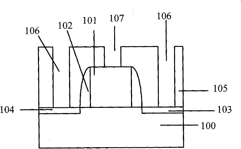
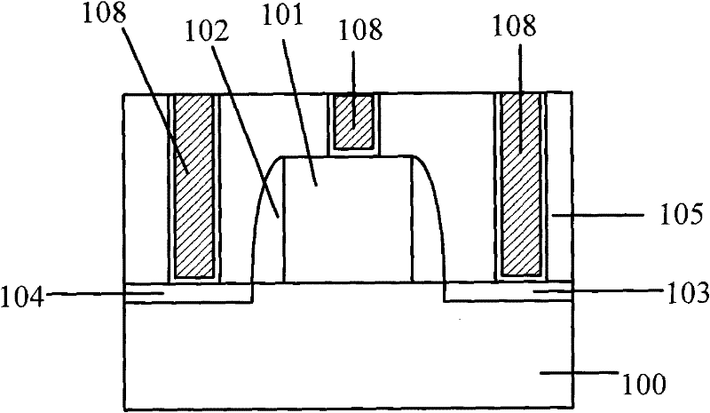
[0039] In the present invention, a first contact hole is formed in the first interlayer dielectric layer on the source electrode and the drain electrode, a second contact hole is formed on the first contact hole, the first metal layer and the first metal layer filled in the first contact hole The second metal layer constitutes a contact plug, which improves the etching precision of etching the first contact hole and the second contact hole, and the resistivity of the second metal layer filled in the second contact hole is smaller than that of the first metal layer , reducing the contact plug resistance of the source and drain of the device.

[0040] Specifically, the present invention provides a method for manufacturing a contact plug. Please refer to Figure 4 , is a schematic flow chart of the method for making the contact plug of the present invention. The methods include:

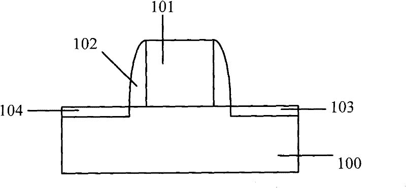
[0041] In step S1, a semiconductor substrate is provided, and a gate structure and a first interl...


PUM


Abstract

The invention provides a method for manufacturing a contact plug. The method comprises the following steps of: providing a semiconductor substrate on which a grid structure and a first interlamination medium layer are formed, wherein the grid structure is flushed with the first interlamination medium layer, and a source and a drain are formed in the semiconductor substrate on two sides of the grid structure; etching the first interlamination medium layer to form a first contact hole which is used for exposing the source and the drain; filling a first metal layer into the first contact hole; forming a second interlamination medium layer on the first interlamination medium layer; etching the second interlamination medium layer to form a second contact hole, wherein the position of the second contact hole corresponds to the position of the first contact hole; and filling a second metal layer into the second contact hole, wherein the resistivity of the second metal layer is smaller than that of the first metal layer; and the second metal layer in the second contact hole and the first metal layer in the first contact hole form the contact plug together. The contact plug manufactured by using the method has small resistance.

Description

technical field [0001] The invention relates to the technical field of semiconductors, in particular to a method for manufacturing a contact plug. Background technique [0002] With the continuous development and progress of semiconductor manufacturing technology and related supporting technologies, the number of devices integrated on a unit area is increasing, and the integration degree of integrated circuits is getting higher and higher. The gap between the gates of adjacent devices becomes Smaller and smaller, which increases the difficulty of device manufacturing. For example, the process of fabricating contact plugs connecting source / drain electrodes and upper metal lines on both sides of gates of adjacent devices becomes more difficult. [0003] Specifically, please refer to Figure 1 to Figure 3 , is a schematic cross-sectional flow chart of a method for manufacturing a contact plug in the prior art. [0004] First, refer to figure 1 , providing a semiconductor su...

Claims


Application Information

Patent Timeline
IPC IPC(8): H01L21/768
Inventor 吴金刚倪景华
Owner SEMICON MFG INT (SHANGHAI) CORP
Why Eureka
Try Eureka