Anti-interference chip packaging structure

A chip packaging structure and chip technology, which is applied in the field of chip packaging structure and new chip packaging structure, can solve the problems of reducing the working stability of electrical equipment, the chip is easily affected by electromagnetic radiation, and disturbing the operating frequency.

Inactive Publication Date: 2012-02-08
常熟市广大电器有限公司
View PDF5 Cites 0 Cited by
  • Summary
  • Abstract
  • Description
  • Claims
  • Application Information

AI Technical Summary

Problems solved by technology

These high-performance chips are easily affected by electromagnetic radiation during operation, which disturbs their operating frequency and reduces the working stability of electrical equipment.

Method used


Image

  • Anti-interference chip packaging structure
  • Anti-interference chip packaging structure

Examples


Embodiment Construction

[0014] The preferred embodiments of the present invention will be described in detail below in conjunction with the accompanying drawings, so that the advantages and features of the present invention can be more easily understood by those skilled in the art, so as to define the protection scope of the present invention more clearly.

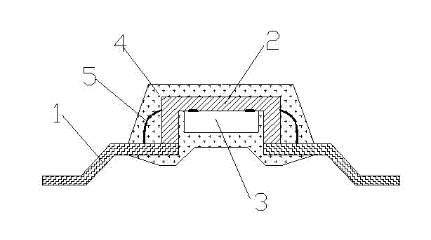
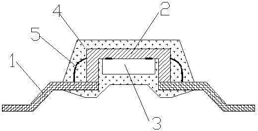
[0015] figure 1 It is a structural schematic diagram of an anti-jamming chip packaging structure in an embodiment of the present invention; the anti-jamming chip packaging structure mainly includes a lead frame 1, a substrate 2, a chip 3 and a package body 4, and it is characterized in that the substrate 2 adopts The "concave" shape structure is placed upside down on the lead frame 1 during packaging, and the chip 3 is flipped on the inner top of the substrate 2, and the two are electrically connected by soldering process.

[0016] In the anti-interference chip packaging structure mentioned in the present invention, glue is used to bond between t...


PUM


Abstract

The invention discloses an anti-interference chip packaging structure, which mainly comprises a pin lead frame, a substrate, a chip and a packaging body. The anti-interference chip packaging structure is characterized in that the substrate is of a concave structure and arranged above the pin lead frame in an inverted mode at the time of package; and the chip is arranged on the top in the substrate in an inserted mode, and the chip is electrically connected with the substrate by adopting a soldering technology. The chip packaging structure disclosed by the invention is simple and convenient for implementation, has good electromagnetic wave radiation resisting capacity and can ensure the high-efficiency operation of the chip; and meanwhile, the chip packaging structure is low in application cost and applied to packaging chips with different specifications and powers.

Description

technical field [0001] The invention relates to a chip packaging structure, in particular to a novel chip packaging structure capable of blocking electromagnetic radiation, and belongs to the technical field of chip packaging. Background technique [0002] In the manufacture of integrated circuits, chips are obtained through the steps of wafer fabrication, forming integrated circuits, and cutting wafers. After the integrated circuit of the wafer is fabricated, the chip formed by dicing the wafer can be electrically connected to the carrier outwardly; wherein, the carrier can be a lead frame or a substrate, and the chip can be wire bonded or covered. The method of crystal bonding is electrically connected to the carrier. If the chip and the carrier are electrically connected by wire bonding, then enter into the manufacturing step of filling the encapsulant to form the chip package. Chip packaging technology is a process technology that wraps the chip to avoid contact betwee...

Claims


Application Information

Patent Timeline
IPC IPC(8): H01L23/04H01L23/06
CPCH01L2224/48091H01L2224/48247H01L2924/00014
Inventor 徐子旸
Owner 常熟市广大电器有限公司
Why Eureka
Try Eureka