
Electrostatic discharge protection module

An electrostatic discharge protection and electrostatic discharge technology, which is applied in the field of electrostatic discharge protection modules, can solve the problems of incorrect operation of a chip, increased electronic devices, or the design and production costs of the chip, and abnormal operation of electronic products.

Inactive Publication Date: 2012-02-08
ILI TECHNOLOGY CORPORATION
View PDF5 Cites 5 Cited by
  • Summary
  • Abstract
  • Description
  • Claims
  • Application Information

AI Technical Summary

Problems solved by technology

This kind of damage will cause permanent or non-permanent (temporary) damage to semiconductor components and computer systems, thus affecting the circuit function of a chip or an electronic product, and making the electronic product work abnormally
[0003] At this stage, the technologies related to electrostatic discharge protection are all aimed at protecting the corresponding registers or latches affected by the electrostatic discharge effect in an electronic device or a chip, such as China Taiwan Patent No. I296439, I300291 , I302374, etc. This technology needs to add corresponding protection circuits to the multiple registers or latches in the electronic device or the chip, which will increase the design and production costs of the electronic device or the chip , and once the electrostatic discharge effect occurs, it can only protect the relevant registers or latches that have been added to the protection circuit design, and for other electronic devices or other circuit components in the chip that are not protected by the protection circuit Unexpected effects may occur, which may cause the electronic device or the chip to perform wrong actions or execute wrong instructions. These are problems that cannot be solved by current technology
[0004] This shows that the above-mentioned existing electrostatic discharge protection obviously still has inconvenience and defects in structure and use, and needs to be further improved urgently.

Method used


Image

  • Electrostatic discharge protection module
  • Electrostatic discharge protection module
  • Electrostatic discharge protection module

Examples


Embodiment Construction

[0034] In order to further explain the technical means and effects of the present invention to achieve the intended purpose of the invention, the specific implementation, structure, characteristics and effects of the electrostatic discharge protection module proposed according to the present invention will be described below in conjunction with the accompanying drawings and preferred embodiments. , as detailed below.

[0035] first preferred embodiment

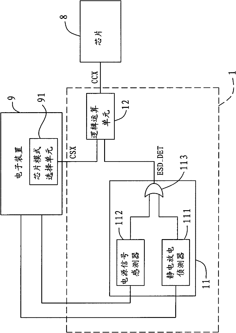
[0036] refer to figure 1 The first preferred embodiment of the electrostatic discharge protection module 1 of the present invention is electrically connected to a chip mode selection unit 91 and a chip 8 of an electronic device 9 respectively, so as to receive a chip mode selection signal output by the chip mode selection unit 9 ( CSX), which is used to switch the current execution mode of the chip 8, which includes: an electrostatic discharge sensing unit 11 and a logic operation unit 12.

[0037] The electrostatic discharg...


PUM


Abstract

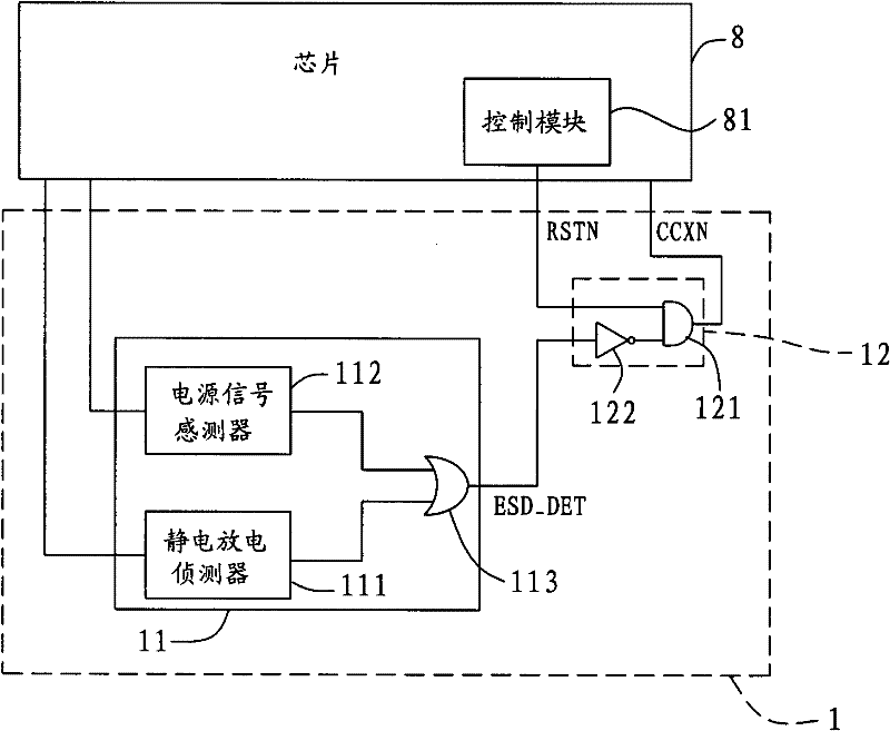
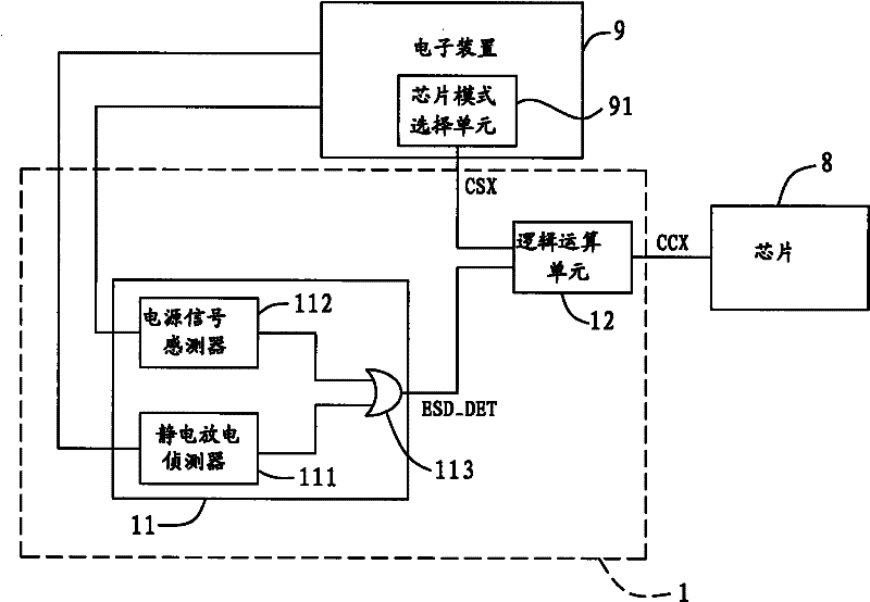
The invention relates to an electrostatic discharge protection module and is applicable to being electrically connected with an electronic device or a chip to detect whether an electrostatic discharge effect is generated in the electronic device or the chip. The electrostatic discharge protection module comprises an electrostatic discharge sensing unit and a logical operation unit, wherein the electrostatic discharge sensing unit is electrically connected with the electronic device or the chip and used for sensing whether the electrostatic discharge effect is generated in the electronic device; and the logical operation unit is electrically connected with the electronic device or the chip and used for performing logical operation and outputting a chip mode control signal into the chip to make the chip switched into an idle mode or a sleep mode.

Description

technical field [0001] The invention relates to an electrostatic discharge protection module, in particular to an electrostatic discharge protection module which prevents the chip from being disturbed by the electrostatic discharge effect from the outside or inside of a chip. Background technique [0002] Generally speaking, the electrostatic discharge (Electrostatic Discharge, ESD) effect is the main factor that causes most electronic components or electronic systems to be damaged by electrical overstress (Electrical Overstress, EOS). This kind of damage will cause permanent or non-permanent (temporary) damage to semiconductor components and computer systems, thereby affecting the circuit function of a chip or an electronic product, and making the electronic product work abnormally. [0003] At this stage, the technologies related to electrostatic discharge protection are all aimed at protecting the corresponding registers or latches affected by the electrostatic discharge ...

Claims


Application Information

Patent Timeline
IPC IPC(8): H02H9/00
Inventor 杨岳霖吴佳政
Owner ILI TECHNOLOGY CORPORATION
Learn More