Circuit board resistance welding processing method

A processing method and circuit board technology, which is applied to the secondary treatment of printed circuits, coating of non-metallic protective layers, etc., can solve the problems of reducing processing time, insufficient solder mask thickness, and shortening the process flow, so as to reduce processing time and improve Bubble removal ability, the effect of solving insufficient solder mask thickness

Inactive Publication Date: 2012-02-22
SHENNAN CIRCUITS
View PDF3 Cites 20 Cited by
  • Summary
  • Abstract
  • Description
  • Claims
  • Application Information

AI Technical Summary

Problems solved by technology

[0004] The embodiment of the present invention provides a circuit board solder resist processing method, which can solve the problems of insufficient solder resist thickness and generation of air bubbles in the solder resist processing of thick copper circuit boards, shorten the process flow, and reduce the processing time

Method used


Image

  • Circuit board resistance welding processing method
  • Circuit board resistance welding processing method

Examples


Embodiment Construction

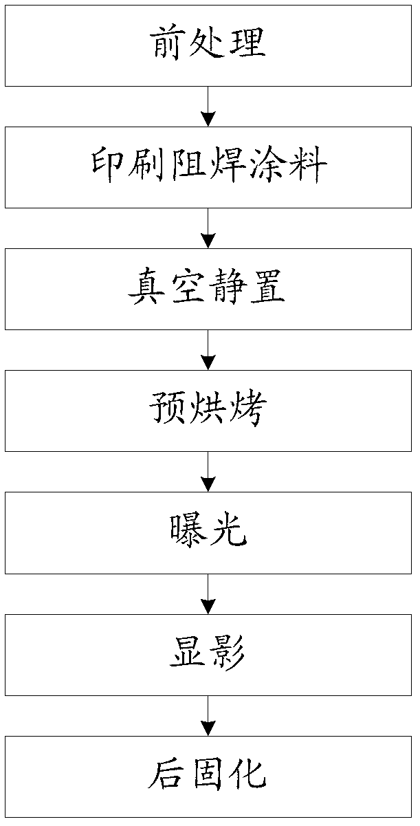
[0008] The embodiment of the present invention provides a solder resist processing method for circuit boards, which adopts the technical solution of standing still in vacuum, which can not only solve the problems of insufficient solder resist thickness and generation of air bubbles in solder resist processing of thick copper circuit boards, but also shorten the solder resistance. Welding process, reducing processing time. A detailed description will be given below in conjunction with the accompanying drawings.

[0009] At present, conventional circuit board solder resist processing methods for thick copper circuit boards usually include two solder resist processes, and each solder resist process includes the following steps:

[0010] Pre-treatment, printing solder mask, standing, pre-baking, exposure, development, post-curing.

[0011] In the first solder mask process, after performing the above-mentioned steps from pre-treatment to post-curing, enter the second solder mask p...


PUM


Abstract

The embodiment of the invention discloses a circuit board resistance welding processing method. The method comprises the steps of pretreatment, resistance welding coating printing, standing, pre-baking, exposure, development and post-curing, wherein the standing step is carried out in vacuum. The method has the following beneficial effects: the bubble elimination capability is improved by adopting vacuum standing; and the problems of insufficient resistance welding thickness and bubble generation during thick copper circuit board resistance welding processing can be solved, the process flow is shortened and the processing time is reduced.

Description

technical field [0001] The invention relates to the technical field of circuit board processing, in particular to a circuit board solder resistance processing method. Background technique [0002] The solder resist processing of thick copper circuit boards with a copper thickness of more than 3 ounces (OZ) is quite difficult. Not only is the processing process long and the time is long, but also due to the large thickness of the copper layer, problems such as insufficient solder resist thickness and bubbles are prone to occur. . [0003] In order to solve the problem of insufficient solder mask thickness and air bubbles, the conventional method is to use multiple solder mask processes to control the printing thickness of the solder mask coating in each process and the rest time after printing to reduce air bubbles and achieve the desired solder mask thickness. Usually, it is necessary to control the printing thickness of the solder resist coating to be less than 60 microns...

Claims


Application Information

Patent Timeline
Patent Type & Authority Applications(China)
IPC IPC(8): H05K3/28
Inventor 冷科刘海龙崔荣罗斌张利华王成勇
Owner SHENNAN CIRCUITS
Why Eureka
Try Eureka