Substrate processing apparatus and substrate processing method

A technology of a substrate processing device and a substrate processing method, which is applied to the device for coating liquid on the surface, transportation and packaging, electrical components, etc., which can solve the problems of reduced component operation rate, difficulty in transportation control, and reduced productivity, so as to achieve suppressed productivity. the reduced effect of

Active Publication Date: 2012-03-21
TOKYO ELECTRON LTD
View PDF7 Cites 2 Cited by
  • Summary
  • Abstract
  • Description
  • Claims
  • Application Information

AI Technical Summary

Problems solved by technology

[0006] However, in one single area among a plurality of single areas that perform the same process, one of the multiple units constituting the multi-unit may be unusable due to failure, maintenance, etc.
At this time, there is such a problem that not only the operation rate of the module is lowered in the single block where the unusable module that cannot be used is generated, so the productivity is lowered, but also when the wafer is sequentially delivered to a plurality of single blocks as described above, In addition, in the structure in which processed wafe

Method used


Image

  • Substrate processing apparatus and substrate processing method
  • Substrate processing apparatus and substrate processing method
  • Substrate processing apparatus and substrate processing method

Examples


Embodiment Construction

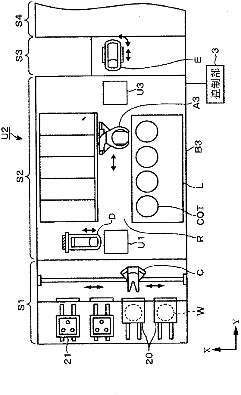
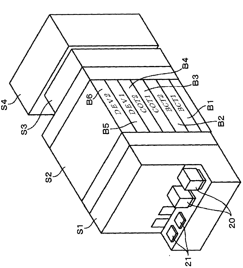
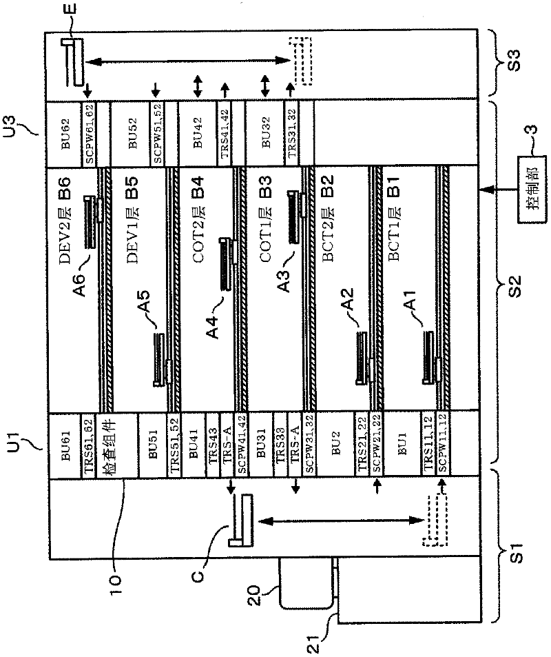
[0068] Next, an example of a resist pattern forming apparatus in which an exposure apparatus is connected to the coating-developing apparatus of the present invention will be briefly described with reference to the drawings. figure 1 It is a plan view showing one embodiment of the above resist pattern forming apparatus, figure 2 It is a schematic perspective view showing one embodiment of the above resist pattern forming apparatus. The device includes a carrying area S1, a processing area S2, a transfer area S3, and an exposure device S4. In the carrying area S1, the transfer arm C takes the wafer W out of the airtight carrier 20 placed on the mounting table 21, and transfers it to the processing area S2 adjacent to the carrying area S1, and the above-mentioned The delivery arm C receives the processed wafer W processed in the processing area S2 and sends it back to the carrier 20 .

[0069] The above-mentioned processing area S2 is constituted by a plurality of, for exampl...


PUM


Abstract

The present disclosure relates to a substrate processing apparatus and a substrate processing method suppressing deterioration of a throughput when a module forming a multi-component is disabled. When a module is disabled, a substrate is provided to a carry-in module capable of placing the wafers most rapidly in the plurality of unit blocks and the substrates are sequentially transported to the module group by the transportation means to be delivered to the carry-out module according to a providing sequence of the substrate to the carry-in module in each of the plurality of unit blocks. In particular, the substrates are extracted from the carry-out module according to a providing sequence of the substrate to the carry-in module and transported to a rear module or a substrate placing part. Thereafter, the substrates are transported to the rear module from the carry-out module or the substrate placing part according to a predetermined sequence in which the substrate is provided to the carry-in module in a normal state.

Description

technical field [0001] The present invention relates to a method for supplying a treatment liquid to the surface of a substrate such as a semiconductor wafer or an LCD substrate (glass substrate for a liquid crystal display) to perform predetermined substrate treatment, such as application of a resist solution, development treatment after exposure, etc. A substrate processing device and a substrate processing method. Background technique [0002] In the photoresist process, which is one of the semiconductor manufacturing processes, a resist is applied to the surface of a semiconductor wafer (hereinafter referred to as a wafer), and the resist is exposed in a predetermined pattern, followed by Develop to form a resist pattern. In the coating-developing apparatus for forming the above-mentioned resist pattern, there is provided a processing section including processing components and the like for performing various processing on a wafer. [0003] As described in, for example...

Claims


Application Information

Patent Timeline
IPC IPC(8): H01L21/67H01L21/677
CPCH01L21/6723H01L21/6715H01L21/67126H01L21/67225B05D5/12
Inventor 宫田亮松山健一郎绪方久仁惠
Owner TOKYO ELECTRON LTD
Why Eureka
Try Eureka