Method for manufacturing active matrix substrate, method for manufacturing organic el display device, and active matrix substrate
A technology of active matrix and manufacturing method, applied in semiconductor/solid-state device manufacturing, semiconductor devices, electrical components, etc., can solve problems such as surface oxidation, and achieve the effect of suppressing the reduction of productivity
- Summary
- Abstract
- Description
- Claims
- Application Information
AI Technical Summary
Problems solved by technology
Method used
Image

Examples
no. 1 approach
[0033] (Brief structure of organic EL display device 1)
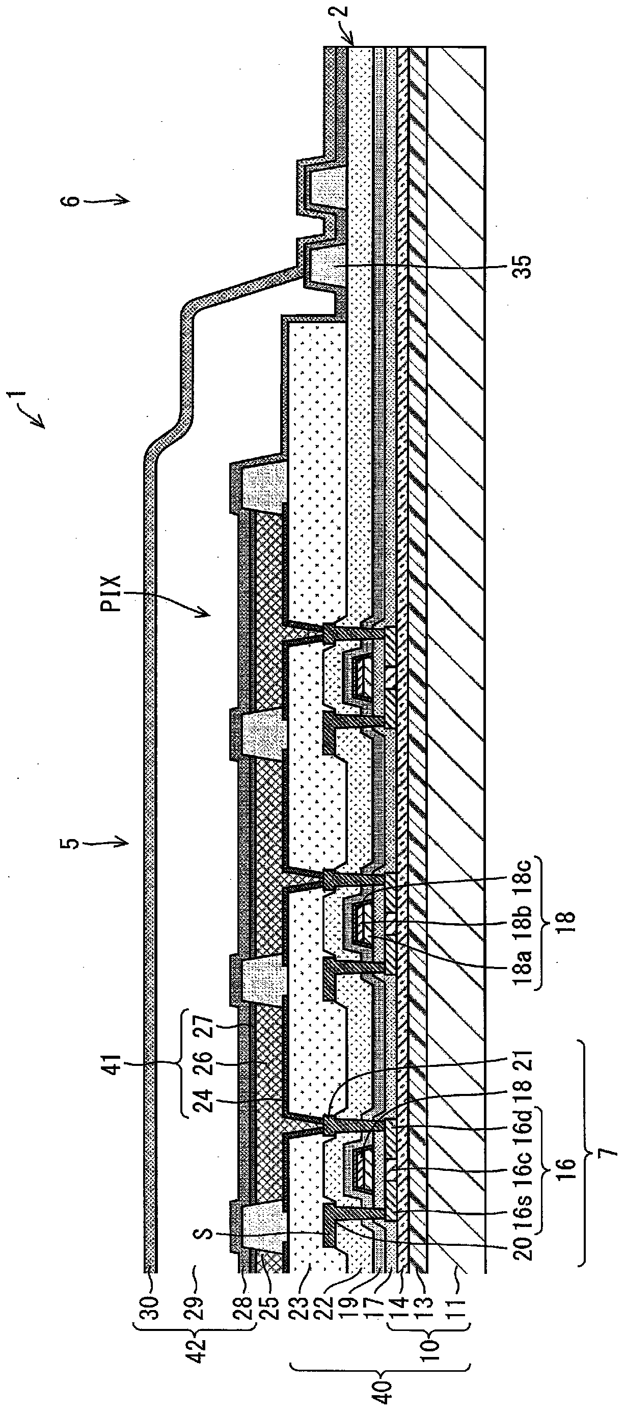
[0034] First, use figure 1 as well as figure 2 A brief structure of the organic EL display device 1 which is an example of a display device using the TFT (Thin Film Transistor) 7 according to the embodiment of the present invention will be described.
[0035] figure 1 It is a cross-sectional view showing the structure of the organic EL display device 1 according to the first embodiment of the present invention. Such as figure 1 As shown, the organic EL display device 1 includes a thin-film-encapsulated (TFE: Thin Film Encapsulation) organic EL substrate 2 and a drive circuit not shown in the figure. The organic EL display device 1 may further include a touch panel.
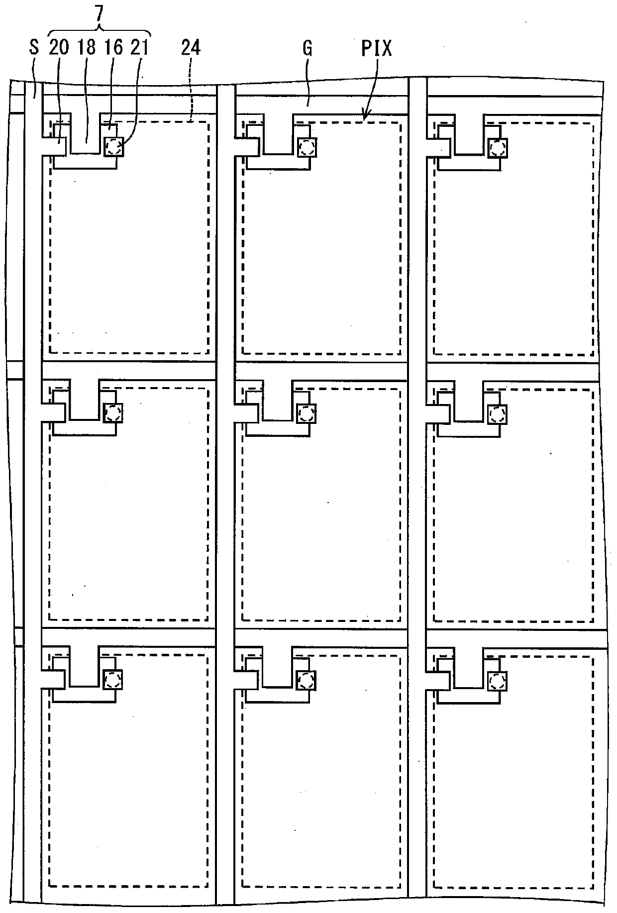
[0036] The organic EL display device 1 has a display area 5 in which pixels PIX are arranged in a matrix and an image is displayed, and a frame area 6 which is a peripheral area surrounding the display area 5 and where no pixels PIX are arranged.
[0037] The org...
no. 2 approach
[0142] If the second embodiment of the present invention is described, it will be as follows. In addition, for convenience of description, members having the same functions as those described in the first embodiment are given the same reference numerals, and descriptions thereof are omitted.
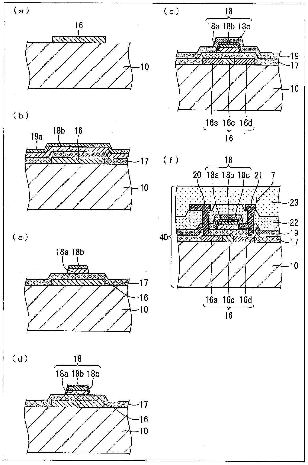
[0143] Figure 8 It is a figure which shows the cross section of the gate electrode of the TFT substrate concerning the 2nd Embodiment of this invention. The gate electrode 18 of the TFT 7 formed on the TFT substrate 40 may also be Figure 8 The structure of the gate electrode 18A.
[0144] The gate electrode 18A has: a first metal film 18a made of molybdenum or molybdenum alloy, a second metal film 18bA laminated on the first metal film 18a made of molybdenum nitride or molybdenum nitride alloy, and a pair of molybdenum oxide or oxide The side surfaces of the first metal film 18a, the side surfaces of the second metal film 18bA, and the third metal film 18cA covering the surface of the moly...
no. 3 approach
[0149] The third embodiment of the present invention will be described as follows. In addition, for convenience of description, members having the same functions as those described in the first embodiment to the second embodiment are given the same reference numerals, and the description thereof is omitted.
[0150] Picture 9 It is a figure which shows the cross section of the gate electrode of the TFT substrate concerning the 3rd Embodiment of this invention. The gate electrode 18 of the TFT 7 formed on the TFT substrate 40 may also be Picture 9 The structure of the gate electrode 18B.
[0151] The gate electrode 18B has a first metal film 18a made of molybdenum or a molybdenum alloy, a second metal film 18bB laminated on the first metal film 18a made of molybdenum oxide or a molybdenum oxide alloy, and a pair of molybdenum oxide or molybdenum oxide alloy. The side surfaces of the first metal film 18a, the side surfaces of the second metal film 18bB, and the third metal film 18...
PUM
 Abstract
Description
Claims
Application Information
 - R&D
- Intellectual Property
- Life Sciences
- Materials
- Tech Scout
- Unparalleled Data Quality
- Higher Quality Content
- 60% Fewer Hallucinations
Browse by: Latest US Patents, China's latest patents, Technical Efficacy Thesaurus, Application Domain, Technology Topic, Popular Technical Reports.
© 2025 PatSnap. All rights reserved.Legal|Privacy policy|Modern Slavery Act Transparency Statement|Sitemap|About US| Contact US: help@patsnap.com