Manufacturing device and manufacturing method

A technology for manufacturing devices and manufacturing methods, which is applied in semiconductor/solid-state device manufacturing, semiconductor devices, electrical components, etc., can solve problems such as increased operating costs, and achieve the goal of suppressing the reduction in productivity, reducing processing load, and suppressing manufacturing costs Effect

Active Publication Date: 2018-10-26
TOWA
View PDF6 Cites 0 Cited by
  • Summary
  • Abstract
  • Description
  • Claims
  • Application Information

AI Technical Summary

Problems solved by technology

Therefore, there is a problem that the running cost when the product is manufactured by cutting (singulation) increases

Method used


Image

  • Manufacturing device and manufacturing method
  • Manufacturing device and manufacturing method
  • Manufacturing device and manufacturing method

Examples


Embodiment 1

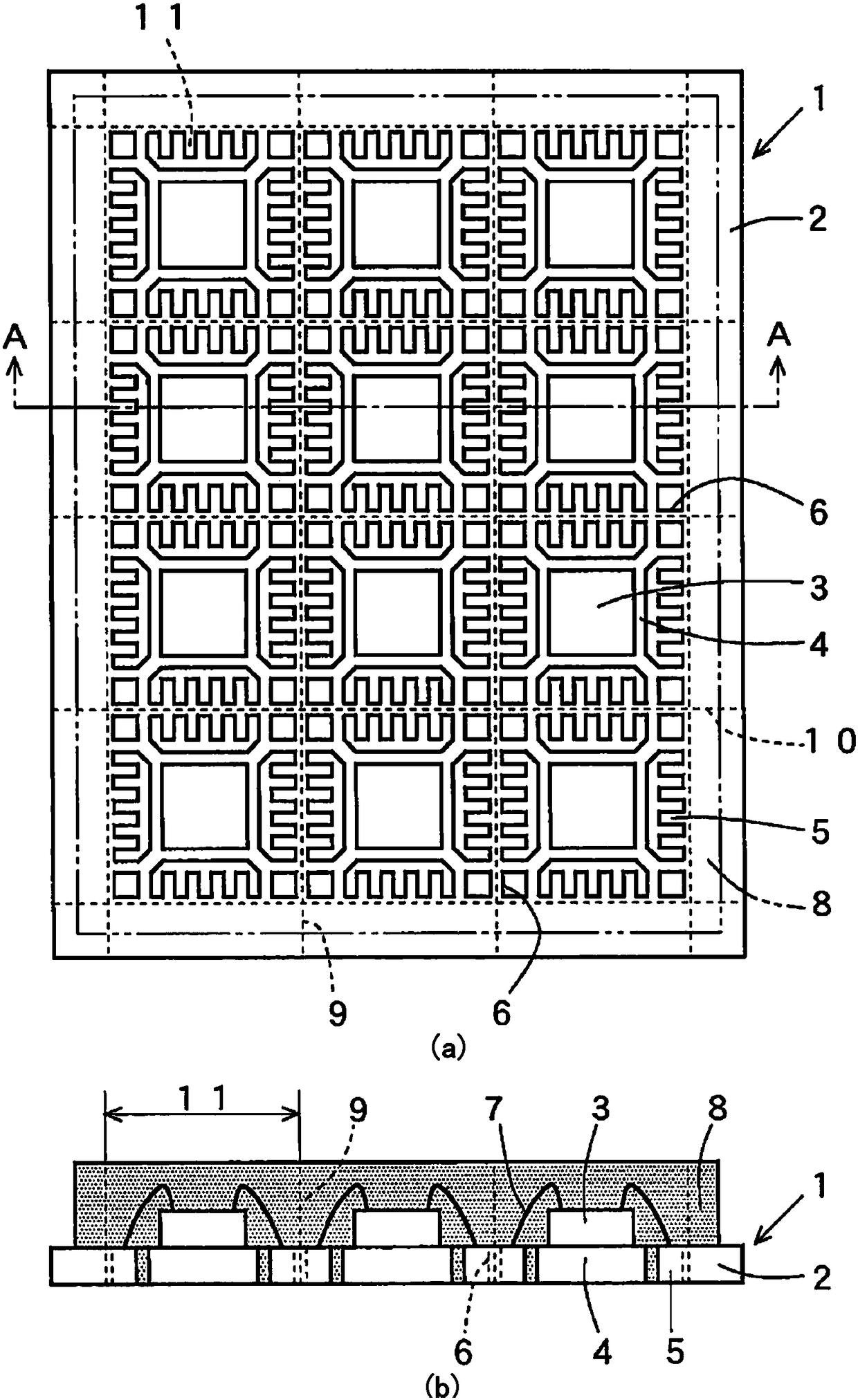
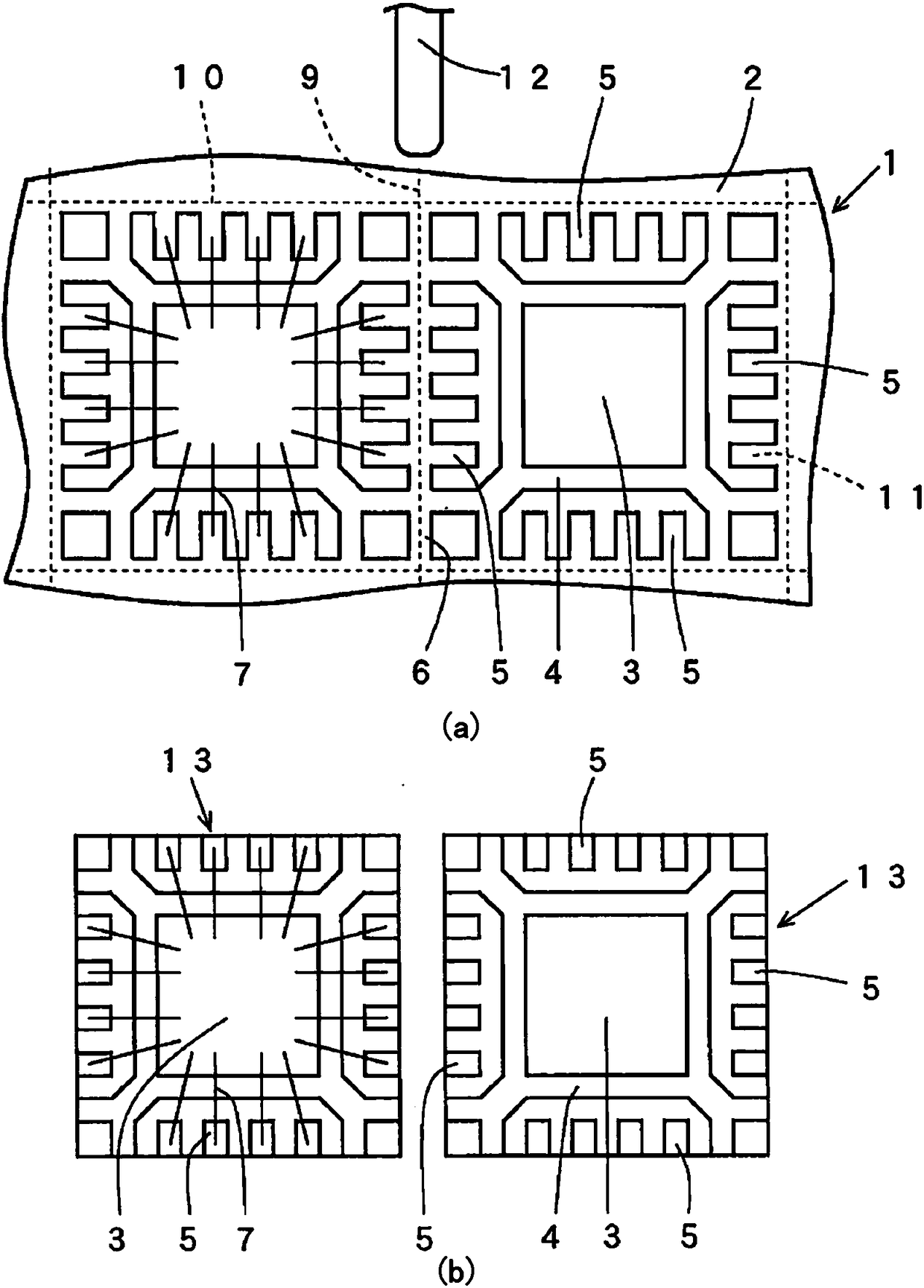
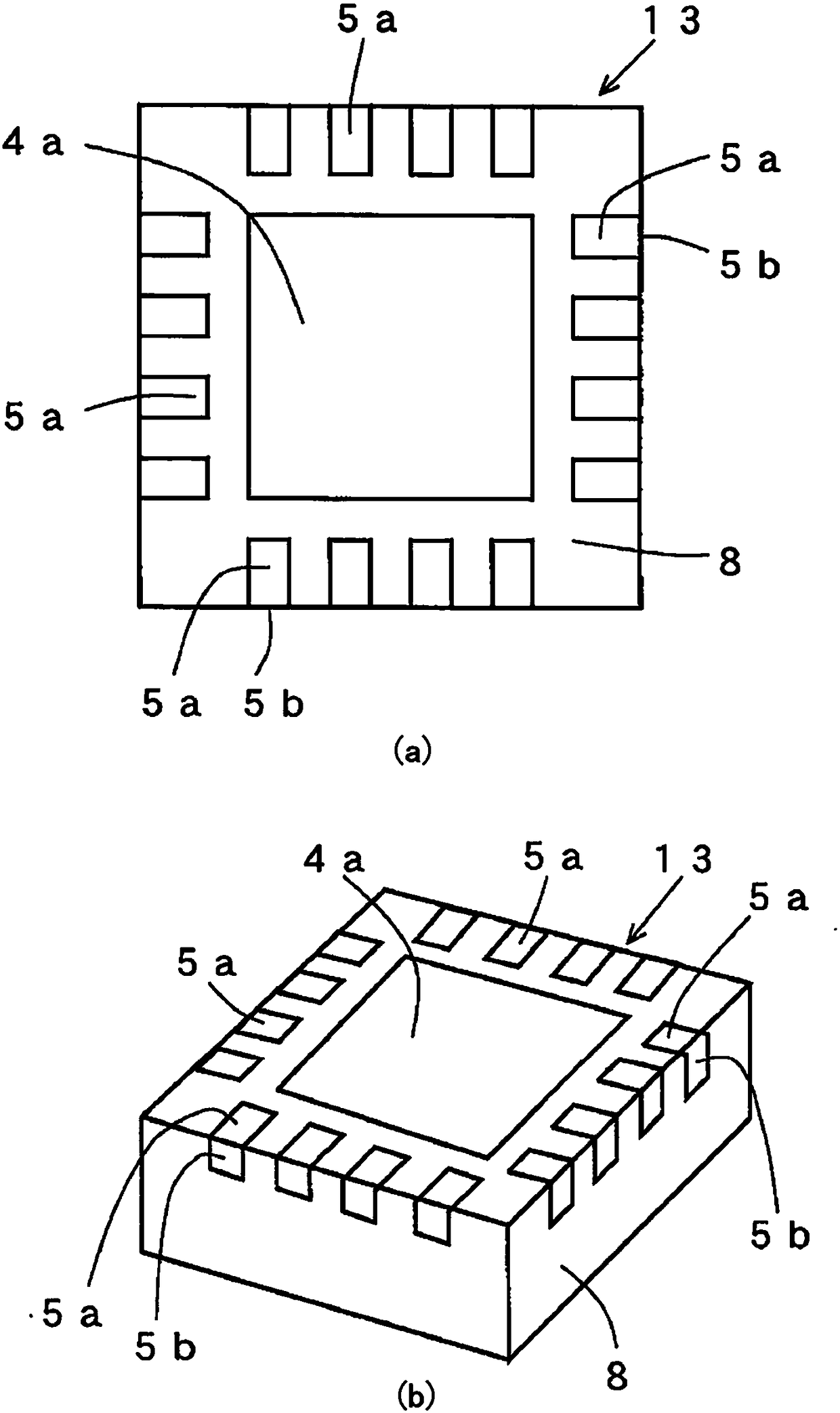
[0042] refer to figure 1 (a)~ Figure 7 (b) Example 1 of the production apparatus of the present invention will be described. For easy understanding, any of the drawings in this application document is appropriately omitted or exaggerated and schematically shown. The same reference numerals are assigned to the same constituent elements, and explanations thereof are appropriately omitted.

[0043] Such as figure 1 of (a), figure 1 As shown in (b), the QFN substrate 1 has a lead frame 2 . Semiconductor chip mounting portions (die pads: Japanese: dipad) 4 for mounting semiconductor chips (functional elements) 3 are arranged in a grid pattern on the lead frame 2 . The lead frame 2 is formed of metal such as copper (Cu) and 42 alloy (Fe—Ni), and its surface is subjected to lead-free tin plating (not shown). Many pins 5 are arranged around each die pad 4 . exist figure 1 of (a), figure 1 In (b), four pins 5 connected to electrodes (not shown) of the semiconductor chip 3 are...

Embodiment 2

[0078] refer to Figure 8 Example 2 of the production apparatus of the present invention will be described. Such as Figure 8 As shown, the manufacturing device 27 is a device for singulating a cut object (multilayer structure) into a plurality of products. The manufacturing apparatus 27 includes a substrate supply module A, a substrate cutting module B, and an inspection module C as respective components. Each component (modules A to C) is detachable and replaceable with respect to other components.

[0079] The substrate supply module A is provided with a substrate supply mechanism 28 . The QFN substrate 1 corresponding to the object to be cut is delivered from the substrate supply mechanism 28 and transferred to the substrate cutting module B by a transfer mechanism (not shown). In the board|substrate supply module A, the control part CTL for setting and controlling the operation|movement of the manufacturing apparatus 27, cutting conditions, etc. is provided.

[0080]...


PUM


Abstract

The invention provides a manufacturing device and a manufacturing method. The QFN substrate is cut in three stages along a plurality of cutting lines set in a grid pattern on the QFN substrate. First, at a cutting line along the longitudinal direction of the QFN substrate, a portion approximately equivalent to the thickness of the tie bar of the lead frame is cut to form a cut groove. Next, the lead frame and the sealing resin are cut together at the cutting line along the width direction of the QFN substrate. Next, a portion corresponding to the thickness of the remaining sealing resin was cut in the cut groove along the longitudinal direction of the QFN substrate. By cutting only the part of the sealing resin in the cutting groove, the processing load when singulating the QFN substrate into QFN products can be finally reduced. Therefore, it is possible to prevent the QFN product from being displaced or scattered from the predetermined position of the jig for cutting.

Description

technical field [0001] The present invention relates to a manufacturing device and a manufacturing method for manufacturing a plurality of products obtained by cutting a cut object and separating the cut object into pieces. Background technique [0002] Divide the substrate including the printed circuit board, lead frame, etc. into a plurality of grid-like areas imaginary, mount chip-shaped elements (such as semiconductor chips) in each area, and then seal the entire substrate with resin, and the components thus formed Called the sealed substrate. The sealed substrate is cut by a cutting mechanism using a rotary knife or the like, and individualized into individual area units to form a product. [0003] Conventionally, a predetermined region of a sealed substrate has been cut using a cutting mechanism such as a rotary knife using a manufacturing apparatus. First, the sealed substrate is placed and sucked on the cutting jig attached to the cutting stage. Next, the sealed s...

Claims


Application Information

Patent Timeline
Patent Type & Authority Patents(China)
IPC IPC(8): H01L21/67
CPCH01L24/97H01L21/67092H01L2224/48091H01L2224/48247H01L2224/97H01L2924/14H01L2224/85H01L2924/00014H01L2924/181H01L2224/49171H01L2924/00012
Inventor 冈本纯
Owner TOWA
Why Eureka
Try Eureka