Sintered ceramic and substrate comprising same for semiconductor device

A technology of sintered body and ceramics, applied in semiconductor devices, semiconductor/solid-state device parts, transportation and packaging, etc., can solve the problems of inability to manufacture DBOC substrates, inability to apply heat dissipation substrates for power modules, low thermal conductivity, etc. Effects of thermal stress relaxation, high mechanical strength, and high thermal expansion coefficient

Inactive Publication Date: 2012-03-28
SUMITOMO METAL SMI ELECTRONICS DEVICES
View PDF8 Cites 19 Cited by
  • Summary
  • Abstract
  • Description
  • Claims
  • Application Information

AI Technical Summary

Problems solved by technology

Therefore, referring to Patent Document 4, it is not possible to manufacture a DBOC substrate for functional modules with few voids generated.
[0042] In addition, the ceramic sintered body disclosed in Patent Document 4 contains zirconia as the main component, so there is a problem that the thermal conductivity is low, and it cannot be applied to a heat dissipation substrate for a power module at all.

Method used


Image

  • Sintered ceramic and substrate comprising same for semiconductor device
  • Sintered ceramic and substrate comprising same for semiconductor device
  • Sintered ceramic and substrate comprising same for semiconductor device

Examples


Embodiment 1

[0120] Hereinafter, the ceramic sintered body according to Example 1 of the present invention will be described.

[0121] The ceramic sintered body according to Example 1 is a ceramic sintered body used as an insulator for a power module substrate used in automobiles, air conditioners, industrial robots, business elevators, household microwave ovens, Electronic equipment such as IH rice cookers, power generation and transmission (wind power generation, solar power generation, fuel cells, etc.), electric railways, UPS (uninterruptible power supply), etc.

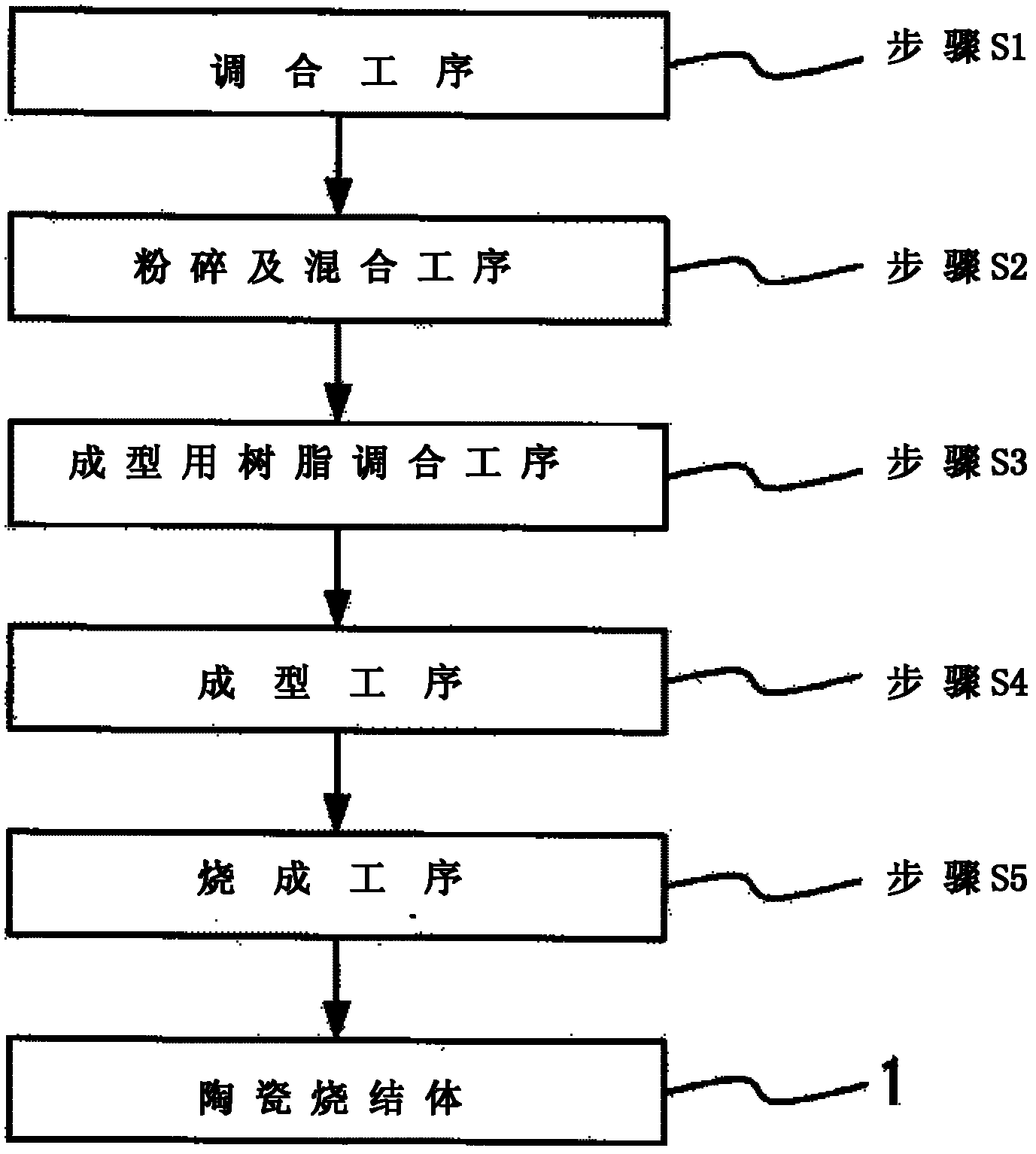
[0122] First, compare figure 1 The method of manufacturing the ceramic sintered body according to Example 1 will be described in detail.

[0123] figure 1 It is a flow chart showing the manufacturing method of the ceramic sintered body concerning Example 1.

[0124] Such as figure 1 As shown, in the production of the ceramic sintered body 1 according to Example 1, first, alumina, partially stabilized zirconia, and magnesi...

Embodiment 2

[0198] Next, a semiconductor device substrate according to Embodiment 2 will be described with reference to FIG. 8 .

[0199] 8( a ) is a cross-sectional view of a semiconductor device substrate according to Example 2, and FIG. 8( b ) is a cross-sectional view of a semiconductor device using the semiconductor device substrate.

[0200] Regarding the semiconductor device substrate 2 according to the second embodiment, the copper plate 4 is disposed on at least a part of the front surface and the back surface of the ceramic substrate 3 composed of the ceramic sintered body 1 according to the above-mentioned first embodiment. More specifically, the copper plate 4 forming the power transmission circuit is arranged on the surface of the flat ceramic substrate 3, and after the flat copper plate 4 is arranged on the back surface of the ceramic substrate 3, it is heated under a nitrogen atmosphere at a temperature of 1070 to 1075°C. After about 10 minutes, a Cu—O eutectic liquid phase...


PUM

PropertyMeasurementUnit
particle sizeaaaaaaaaaa

Abstract

A sintered ceramic which has a high mechanical strength and excellent heat dissipation properties and which, when bonded to a copper sheet, is less apt to generate voids at the interface therebetween. The sintered ceramic (1) is for use as an insulating substrate on which an electronic component is to be mounted. The sintered ceramic is characterized by being produced from a powder material comprising alumina as the main component, partially stabilized zirconia, and magnesia, the upper limit of the content of the partially stabilized zirconia being 30 wt.% relative to the total weight of the powder material, and the content of the magnesia being in the range of 0.05-0.50 wt.% relative to the total weight of the powder material. The sintered ceramic is further characterized in that 80-100% of the zirconia crystals contained in the sintered ceramic have a tetragonal phase.

Description

technical field [0001] The present invention relates to a ceramic sintered body and a substrate for a semiconductor device using the ceramic sintered body. The ceramic sintered body is used on a substrate for a semiconductor device used in a power transistor module, etc., and particularly relates to a surface of a ceramic substrate composed of a ceramic sintered body. A DBOC substrate (Direct Bonding of Copper Substrate) in which a copper plate is mounted, or a DBOA substrate (Direct Bonding of Aluminum substrate) in which an aluminum plate is mounted on the surface of a ceramic substrate. Background technique [0002] Substrates used in substrates for power semiconductor devices are required to have high mechanical strength and excellent thermal conductivity, and ceramic substrates are used as insulators that satisfy these conditions. [0003] As we all know, generally speaking, ceramic substrates include alumina ceramic substrates with alumina as the main component, al...

Claims


Application Information

Patent Timeline
Patent Type & Authority Applications(China)
IPC IPC(8): C04B35/111C04B35/44H01L23/13H01L23/14
CPCC04B2237/704C04B2235/785C04B2237/343H01L2224/48227C04B2237/54H01L2924/01004C04B2235/3225C04B2235/3246C04B2235/80C04B2235/9607H01L2924/01012C04B2235/3206C04B2235/3222H01L2224/48091H01L2924/01057C04B37/021H01L23/15C04B2237/402C04B2235/786C04B2235/3418H01L2924/01019C04B35/119C04B37/025H01L2924/01322H01L2224/32225C04B2237/86H01L24/48H01L2224/73265C04B2235/96C04B2237/06C04B2235/77C04B2235/656H01L23/3735C04B2237/706H01L2924/09701C04B2237/407H01L24/73H01L2924/00014H01L2924/181Y10T428/256H01L2924/00012H01L2224/45099H01L2224/45015H01L2924/207H01L2924/00C04B35/01C04B35/03C04B35/10C04B35/111C04B35/48H01L23/13H01L23/14
Inventor 长广雅则大上纯史小松敬幸
Owner SUMITOMO METAL SMI ELECTRONICS DEVICES
Why Eureka
Try Eureka