Halogen-resistant, anodized aluminum for use in semiconductor processing apparatus

a technology of anodized aluminum and semiconductor processing equipment, which is applied in the direction of vacuum evaporation coating, sputtering coating, coating, etc., can solve the problems of reducing the performance life affecting the performance of anodized semiconductor equipment, etc., to achieve the effect of improving the abrasion resistance, improving the density of the present oxidized film, and improving the performance lifetime of the anodized semiconductor equipmen

Inactive Publication Date: 2006-05-23
APPLIED MATERIALS INC
View PDF23 Cites 15 Cited by
  • Summary
  • Abstract
  • Description
  • Claims
  • Application Information

AI Technical Summary

Benefits of technology

[0025]The particular combination of process variables described above also produces an oxidized aluminum layer which is more densely packed and more uniform than previously known in the art. For example, the size of the internal pores (shown as 314 on FIG. 3C) within the hexagonal cells of the oxidized aluminum film of the present invention range in size from about 300 Å to about 700 Å. This is compared with previously known oxidized aluminum films, where the pore size varied from about 100 Å to about 2000 Å in diameter. As a result, the density of the present oxidized film is generally higher, providing improved abrasion resistance. Depending on the application, the normal range of the anodized film thickness ranges between about 0.7 mils to about 2.5 mils (18 μm to 63 μm).
[0026]Although the above anodiza

Problems solved by technology

In addition, since the processes used to create the integrated circuits leave contaminant deposits on the surfaces of the processing apparatus, such deposits are commonly removed using plasma cleaning techniques which employ at least one halogen-containing gas.
However, aluminum is susceptible to reaction with halogens such as chlorine, fluorine, and bromine, to produce, for example, AlCl3; Al2Cl6; AlF3; or AlBr3.
The aluminum-fluorine compounds can flake off the surfaces of process apparatus parts, causing an eroding away of the parts themselves, and serving as a source of particulate contamination of the process chamber (and parts produced in the chamber).
This creates voids in the structure which render the structure unstable and produce a surface having questionable integrity.
Despite the use of anodized alumina protective layers, the lifetime of anodized aluminum parts in semiconductor processing apparatus, such as susceptors in CVD reactor chambers, and gas distribution plates for etch process chambers has been limited, due to the gradual degradation of the protective anodized film.
Failure of the protective anodized film leads to excessive particulate generation within the reactor chamber, requiring maintenance downtime for replacing the failed aluminum parts and for cleaning particulates from the rest of the chamber.
For example, if the alloy is too soft, it is difficult to drill a hole, as material tends to stick during the drilling rather

Method used


Image

  • Halogen-resistant, anodized aluminum for use in semiconductor processing apparatus
  • Halogen-resistant, anodized aluminum for use in semiconductor processing apparatus
  • Halogen-resistant, anodized aluminum for use in semiconductor processing apparatus

Examples


Embodiment Construction

[0034]As a preface to the detailed description, it should be noted that, as used in this specification and the appended claims, the singular forms “a”, “an”, and “the” include plural referents, unless the context clearly dictates otherwise.

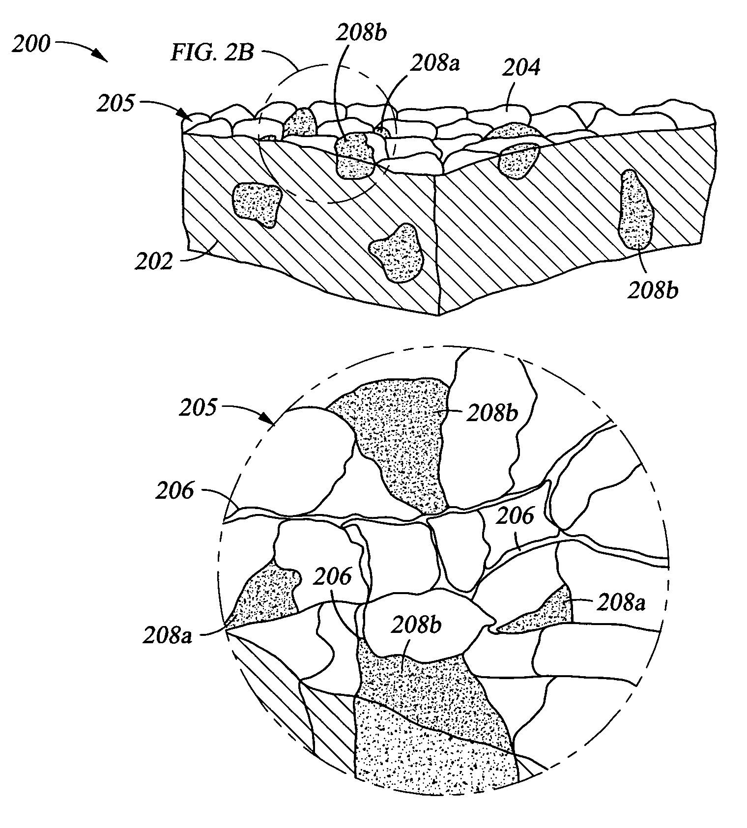
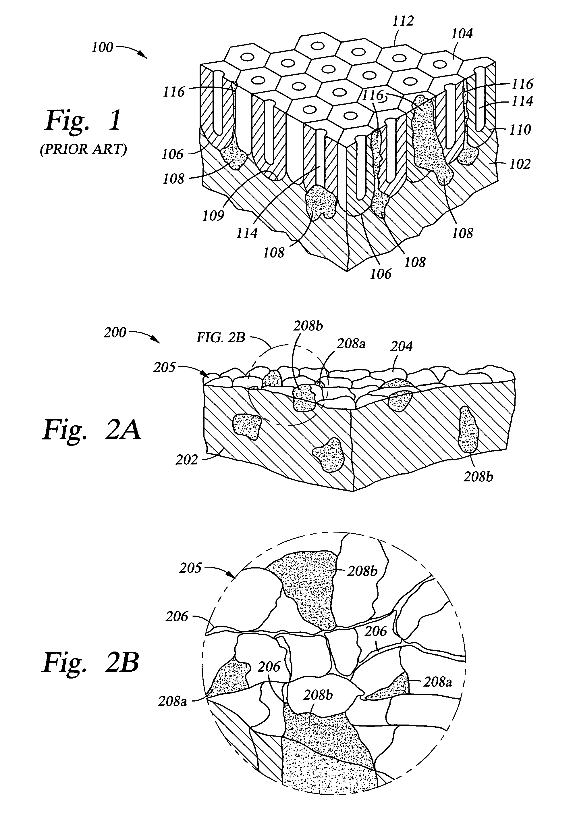
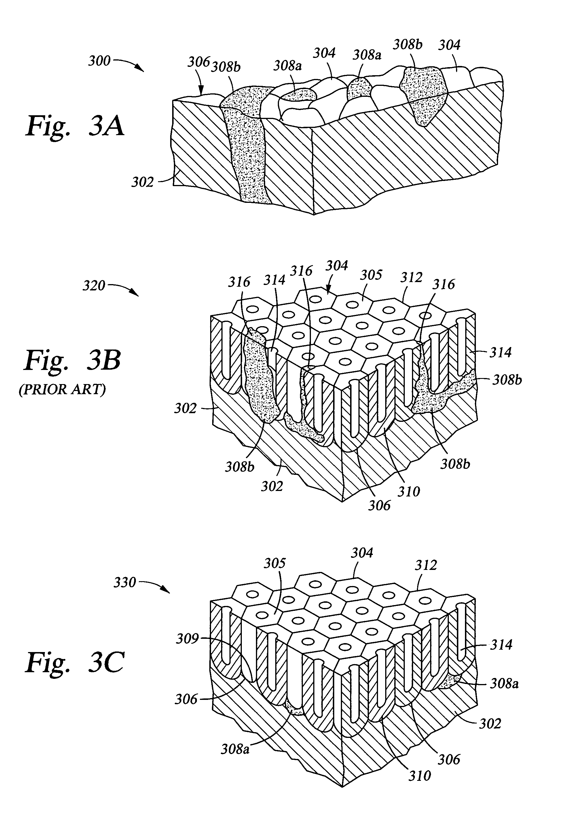
[0035]The objective of the present invention is to provide a semiconductor processing apparatus which is resistant to corrosive processing conditions. In general, the body of the apparatus is formed from an aluminum alloy. To enable the aluminum alloy to resist corrosion, an aluminum oxide protective film is applied over a surface of the aluminum alloy which is to be exposed to the corrosive processing environment. To obtain the best corrosion resistance and longest acceptable performance lifetime for the apparatus article, the article is fabricated in a particular manner. As described above, for best results, the aluminum alloy used for the body of the article should be formed from a specialized halogen-resistant aluminum alloy of the kind descri...


PUM

PropertyMeasurementUnit
Temperatureaaaaaaaaaa

Abstract

We have discovered that the formation of particulate inclusions at the surface of an aluminum alloy article, which inclusions interfere with a smooth transition from the alloy surface to an overlying aluminum oxide protective film can be controlled by maintaining the content of mobile impurities within a specific range and controlling the particulate size and distribution of the mobile impurities and compounds thereof; by heat-treating the aluminum alloy at a temperature less than about 330° C.; and by creating the aluminum oxide protective film by employing a particular electrolytic process. When these factors are taken into consideration, an improved aluminum oxide protective film is obtained.

Description

BACKGROUND OF THE INVENTION[0001]1. Field of the Invention[0002]In general, the present invention relates to a method of fabrication of semiconductor processing apparatus from an aluminum substrate. In particular, the invention relates to a structure which provides a particular interface between an aluminum surface and aluminum oxide overlying that surface. The invention also relates to a method of producing the interfacial structure.[0003]2. Brief Description of the Background Art[0004]Semiconductor processing involves a number of different chemical and physical processes whereby minute integrated circuits are created on a substrate. Layers of materials which make up the integrated circuit are created by chemical vapor deposition, physical vapor deposition and epitaxial growth, for example. Some of the layers of material are patterned using photoresist masks and wet and dry etching techniques. Patterns are created within layers by the implantation of dopants at particular locations...

Claims


Application Information

Patent Timeline
IPC IPC(8): C25D3/04C22C21/00C25D11/04C25D11/06C25D11/16
CPCC25D11/04C25D11/045C25D11/16C22C21/06C25D11/08
Inventor LIN, YIXINGWEST, BRIAN T.WANG, HONGWU, SHUN JACKSONSUN, JENNIFER YSTOW, CLIFFORD C.THACH, SENH
Owner APPLIED MATERIALS INC
Why Eureka
Try Eureka