
High-power LED (light-emitting diode) light source packaging structure manufactured by graphene and production process thereof

A technology of LED light source and packaging structure, which is applied in the direction of electrical components, circuits, semiconductor devices, etc., to achieve the effects of easy promotion and application, efficient heat conduction, and large volume

Inactive Publication Date: 2012-04-11
杭州创元光电科技有限公司
View PDF5 Cites 13 Cited by
  • Summary
  • Abstract
  • Description
  • Claims
  • Application Information

AI Technical Summary

Problems solved by technology

[0004] Aiming at the deficiencies in the existing high-power LED light source technology, the present invention proposes a high-power LED light source packaging structure made of graphene and its production process using graphene as the material of the LED light source substrate and chip carrying area.

Method used


Image

  • High-power LED (light-emitting diode) light source packaging structure manufactured by graphene and production process thereof
  • High-power LED (light-emitting diode) light source packaging structure manufactured by graphene and production process thereof
  • High-power LED (light-emitting diode) light source packaging structure manufactured by graphene and production process thereof

Examples


Embodiment Construction

[0026] In order to make the advantages and technical solutions of the present invention more clear, further descriptions will be made below in conjunction with the accompanying drawings.

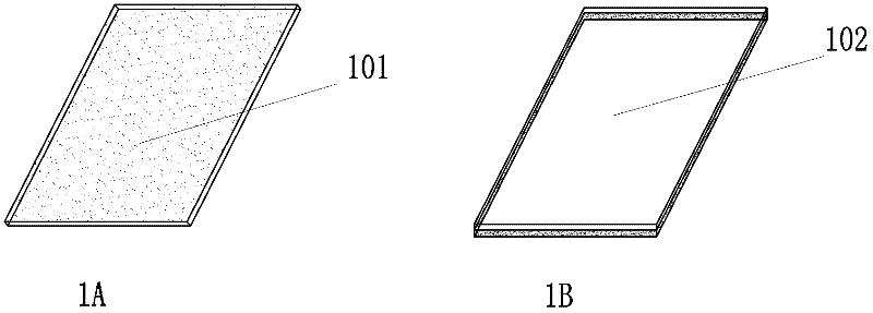
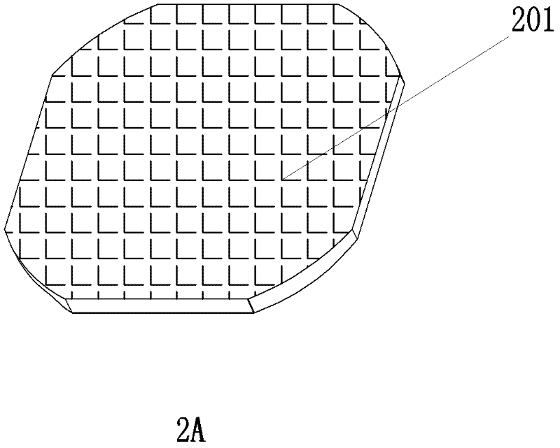
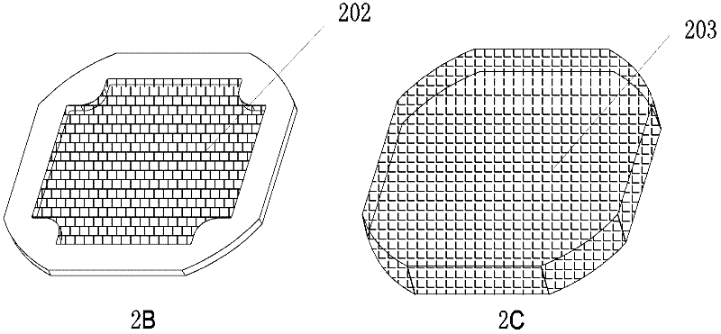
[0027] refer to figure 1 , figure 2 , image 3 , using graphene as the LED light source substrate and chip carrying area material to make a 50W LED light source.

[0028] The LED light source is composed of three parts: a light source substrate 12 , a surrounding frame 11 , and a chip carrying area 10 . The chip carrying area can directly use the surface-treated sheet-shaped graphene carrying sheet 101 , or use copper-based graphene 102 .

[0029] Such as Figure 2A and figure 2 B. figure 2 As shown in C, the light source substrate adopts the light source substrate 201 that conforms to the shape requirements by covering and bonding graphene on the surface of other easy-to-form flame-retardant materials by means of spraying, electroplating, vacuum coating or vacuum sputtering.

[00...


PUM


Abstract

The invention discloses a high-power LED (light-emitting diode) light source packaging structure manufactured by graphene and production process thereof, and relates to high-power LED light source packaging. At present, the area and weight of a baseplate are added to accelerate heat dissipation for a high-power LED, the light source volume of the whole high-power LED is increased, weight is increased, LED light source cost is improved, and meanwhile the advantages such as, portability and the like of the LED are lost, thereby being difficult to apply. The high-power LED light source packaging structure provided by the invention comprises a baseplate which is fixedly connected with at least one chip and electrically connected with the chip, and the high-power LED light source packaging structure is characterized in that a single layer graphene material is covered on at least one of the upper surface and lower surface of the baseplate; the baseplate surface in a chip loaded region uses single layer flake graphene as a heat conduction, radiating material, the physical characteristic of the graphene is fully utilized, the heat energy generated by the chip when the high-power LED light source is conducted so as to diffuse; and under the condition of not increasing the light source weight and volume, the operating temperature of the chip is obviously improved.

Description

technical field [0001] The invention relates to the application of graphene, in particular to a novel LED light source produced by using graphene as the material of the LED light source substrate and the chip carrying area. Background technique [0002] Due to the advantages of LED as a light source itself, LED light sources have played an increasingly important role in the field of functional lighting. Current LED light sources use metals with high thermal conductivity as substrates, the most common being copper or aluminum. By fixing the chip on the copper or aluminum plate, the heat generated by the chip is dissipated to the heat sink through the copper or aluminum. For high-power LEDs, heat dissipation is accelerated by increasing the area and weight of the substrate. This method of increasing the area and weight of the substrate often increases the volume and weight of the entire high-power LED light source, increases the cost of the LED light source, and at the same ...

Claims


Application Information

Patent Timeline
Patent Type & Authority Applications(China)
IPC IPC(8): H01L33/00
Inventor 王铨海郭邦俊楼满娥
Owner 杭州创元光电科技有限公司
Learn More