Blue-light-excited TFT (thin film transistor)-LED (light emitting diode) array display substrate and manufacturing method thereof

A technology of TFT-LED and array display substrate, which is applied in semiconductor/solid-state device manufacturing, electrical components, electric solid-state devices, etc. It can solve the problems of high production cost, poor color uniformity, and low resolution, and achieve easy large-scale industrialization , improve heat dissipation, and improve product performance

Inactive Publication Date: 2012-05-02
GUIZHOU UNIV
View PDF6 Cites 9 Cited by
  • Summary
  • Abstract
  • Description
  • Claims
  • Application Information

AI Technical Summary

Problems solved by technology

However, the currently used splicing forms of LED displays have disadvantages such as low resolution, poor color uniformity, and large volume. The coordination and consistency of different splicing parts of the LED display are difficult to guarantee, the production cost is relatively high, and the heat dissipation design of high-power devices is difficult. , only applicable to problems such as large-screen display, which limits the further development of splicing LED color display devices

Method used


Image

  • Blue-light-excited TFT (thin film transistor)-LED (light emitting diode) array display substrate and manufacturing method thereof
  • Blue-light-excited TFT (thin film transistor)-LED (light emitting diode) array display substrate and manufacturing method thereof
  • Blue-light-excited TFT (thin film transistor)-LED (light emitting diode) array display substrate and manufacturing method thereof

Examples


Embodiment Construction

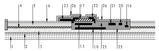
[0082] A blue light excitation TFT-LED array display substrate structure of the present invention is as follows Figure 24As shown, above the substrate 1 are the buffer layer 2 and the n-type GaN layer 3 in sequence; on the n-type GaN layer 3 is the blue light emitting layer 4, and on the blue light emitting layer are the p-type GaN layer 5 and the transparent electrode in sequence Layer 6. The n-type GaN layer 3, the blue light-emitting layer 4, the p-type GaN layer 5 and the transparent electrode layer 6 together form a display unit. A control area 7 is provided on the display unit, and a lead area 8 is provided between the display units. In the control area 7, there is a capacitor composed of the lower plate 10 of the capacitor, the upper plate 12 of the capacitor, and the insulating layer 25 between the upper and lower plates. A working TFT composed of a working TFT gate 13, a working TFT channel 17, a working TFT source 22, a working TFT drain 23 and an intermediate insu...


PUM


Abstract

The invention discloses a blue-light-excited TFT (thin film transistor)-LED (light emitting diode) array display substrate and a manufacturing method thereof. A semiconductor integrating technique is utilized to integrate double TFTs and a blue LED unit on one substrate; blue-light-excited fluorescent powder is utilized to implement white light emission; and a color film technology is utilized to implement blue-light-excited TFT-LED array display. Two TFTs and a capacitor are integrated on each isolated light-emitting array unit as a control circuit of the light emitting unit; a fluorescent powder layer is covered on the array substrate, and a color film substrate matched with the array substrate is covered on the fluorescent powder layer; or the fluorescent powder layer and the color film substrate are integrated, and the color film substrate is directly covered on the array substrate. The substrate disclosed by the invention can overcome the defects in the existing LED and LCD (liquid crystal display) display to some extent, and greatly enhance the display quality and display effect; and the manufacturing method is compatible with the existing semiconductor technique, and can easily implement industrialization.

Description

technical field [0001] The invention relates to an LED array display substrate and a manufacturing method thereof, in particular to a blue light excitation TFT-LED array display substrate structure and a manufacturing method thereof. Background technique [0002] With the continuous improvement of people's material and cultural living standards, people's requirements for display technology are also getting higher and higher. Display technology is gradually developing towards flat panel, small size, light weight, low power consumption and other aspects. Due to the advantages of small size, low radiation and low power consumption, liquid crystal display has been developed rapidly and has become the mainstream of current display technology, gradually replacing traditional CRT display technology in many application fields. However, the response speed of the liquid crystal display is relatively slow, and there are still many deficiencies in color reproduction. With the successf...

Claims


Application Information

Patent Timeline
Patent Type & Authority Applications(China)
IPC IPC(8): H01L27/15H01L21/77
Inventor 邓朝勇杨利忠胡绍璐杨小平雷远清
Owner GUIZHOU UNIV
Why Eureka
Try Eureka