Supercharge Your Innovation With Domain-Expert AI Agents!

Hall device error compensation circuit

A Hall device and error compensation technology, which is applied in the field of Hall device error compensation circuit, can solve problems such as inaccurate detection, uneven resistivity of Hall devices, and unequal output terminals.

Active Publication Date: 2012-05-09
BEIJING SHUOKE ZHONGKEXIN ELECTRONICS EQUIP CO LTD
View PDF5 Cites 11 Cited by
  • Summary
  • Abstract
  • Description
  • Claims
  • Application Information

AI Technical Summary

Problems solved by technology

Since the resistivity, mobility and carrier concentration of the Hall device material change with the temperature, the performance parameters of the Hall device must change with the temperature, resulting in a change in the Hall potential and a temperature error; The Hall electrodes are symmetrically welded on both sides of the Hall device, so that the two electrode points cannot be completely located on the same equipotential surface. In addition, the resistivity of the Hall device is not uniform or the excitation terminal is in poor contact, resulting in unequal potential at the output terminal. electric potential
As a result, the detection is inaccurate and the magnetic field is unstable.

Method used


Image

  • Hall device error compensation circuit
  • Hall device error compensation circuit
  • Hall device error compensation circuit

Examples


Embodiment Construction

[0018] Attached below figure 1 The specific embodiments will further introduce the present invention, but not as a limitation to this patent.

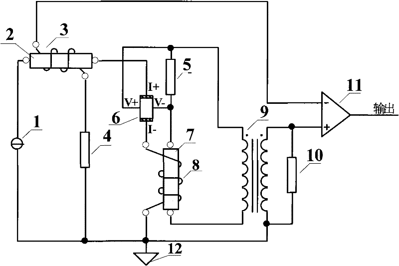
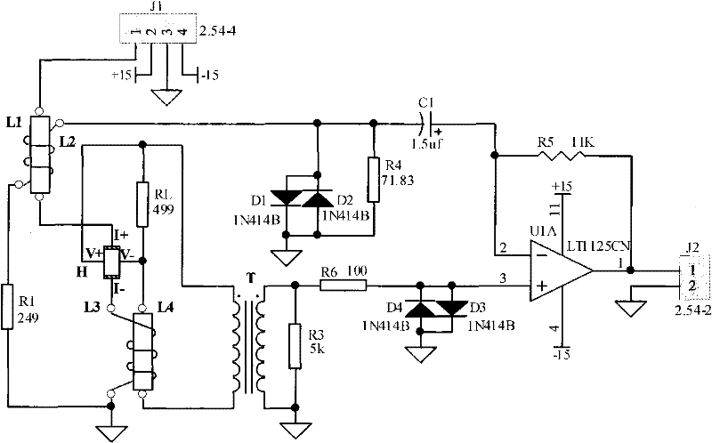
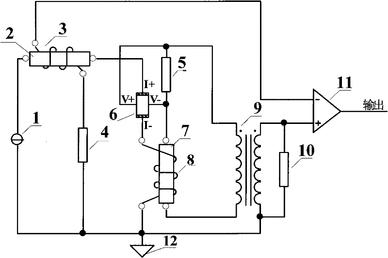
[0019] figure 2 It is a schematic diagram of a specific embodiment of the Hall device error compensation circuit, which includes 2 connectors, 2 inductors with temperature coefficients, 2 wire-wound inductors, 5 resistors, 4 diodes and a component, etc., which are countless Many components are organically combined to form a simple and reliable Hall device error compensation circuit.

[0020] Its specific working principle is as follows:

[0021] The ±15V working power supply, ground and constant AC signal required by the circuit are all introduced from the connector J1. Place the Hall device 6 in the magnetic field to be detected. In order to prevent poor contact of the electrodes of the Hall device 6, the excitation terminal and the output terminal of the Hall device are directly completed by welding.

[0022] The constant AC sig...


PUM


Abstract

The invention relates to a Hall device error compensation circuit, which comprises a constant alternating current source 1, an inductor 2, a wire wound inductor 3, a corrected resistor 4, a load resistor 5, a Hall device 6, an inductor 7, a wire wound inductor 8, a transformer 9, a resistor 10, an amplifier 11 and a grounding terminal 12. The circuit is connected with the load resistor 5 in parallel to compensate temperature error, and adopts a compensation device coupling inductor formed by the inductor 2 and the wire wound inductor 3 to enable the temperature error to reach the optimum effect; and in addition, a coupling inductor comprising the inductor 7 and the wire wound inductor 8 is connected onto an excitation end and an output end of the Hall device 6 in parallel to compensate zero error of the Hall device 6, so that an inequipotential electric potential is minimized. The circuit provided by the invention is simple, has good time response, and automatically compensate temperature drift and the zero error of the Hall device carrying out magnetic field detection, so that the compensation is more accurate and reliable.

Description

technical field [0001] The invention relates to a Hall device error compensation circuit, in particular to an error compensation circuit for detecting magnetic fields in an ion implanter for manufacturing semiconductor devices. Background technique [0002] With the increasing integration of semiconductor devices, the wafer size is getting bigger and bigger, and the unit device size is getting smaller and smaller, which puts forward higher requirements for various semiconductor process equipment. In an ion implanter, the ions generated by the ion source through discharge are mixed ions of various ions. The ions implanted into the wafer require a single pure ion, so the required ion species must be sorted out. The sorting principle is to use the Luotian magnetic force, that is, the trajectory (R) of the charged particles in the constant magnetic field (B) and the mass of the charged particles (m), the energy of the charged particles (E) and the number of charges satisfy the ...

Claims


Application Information

Patent Timeline
Patent Type & Authority Applications(China)
IPC IPC(8): G01R33/07
Inventor 唐景庭伍三忠孙勇彭彬彭立波
Owner BEIJING SHUOKE ZHONGKEXIN ELECTRONICS EQUIP CO LTD
Features
  • R&D
  • Intellectual Property
  • Life Sciences
  • Materials
  • Tech Scout
  • Unparalleled Data Quality
  • Higher Quality Content
  • 60% Fewer Hallucinations
Learn More