Check patentability & draft patents in minutes with Patsnap Eureka AI!

Memory element and flash memory array reading and operating method and structures thereof

A memory element and memory array technology, applied in static memory, read-only memory, information storage, etc., can solve the problems of affecting the continuous range, reading errors, shortening the length of word lines, etc.

Active Publication Date: 2015-01-07
TAIWAN SEMICON MFG CO LTD
View PDF5 Cites 0 Cited by
  • Summary
  • Abstract
  • Description
  • Claims
  • Application Information

AI Technical Summary

Problems solved by technology

For split gate flash memory devices, shortening the word line length results in higher channel current leakage and increased bit errors
If the channel length is increased in order to improve channel current leakage, it will cause a drop in read current during erase operations and affect the endurance window after operating cycles.
Additionally, current leakage can cause errors in reading

Method used


Image

  • Memory element and flash memory array reading and operating method and structures thereof
  • Memory element and flash memory array reading and operating method and structures thereof
  • Memory element and flash memory array reading and operating method and structures thereof

Examples


Embodiment Construction

[0041] The content disclosed in the present invention provides many different embodiments or examples, and different technical features applied in different embodiments can be understood after reading this specification. The content and practice of specific embodiments will be described below to simplify the disclosure of the present invention. Of course, these examples are not intended to limit the present invention. In addition, in different embodiments, the present invention may reuse the same index numbers and / or words. The purpose of using these reference numbers and / or words is to simplify and clarify the present invention, but not to indicate that different embodiments and / or disclosed structures must have the same features.

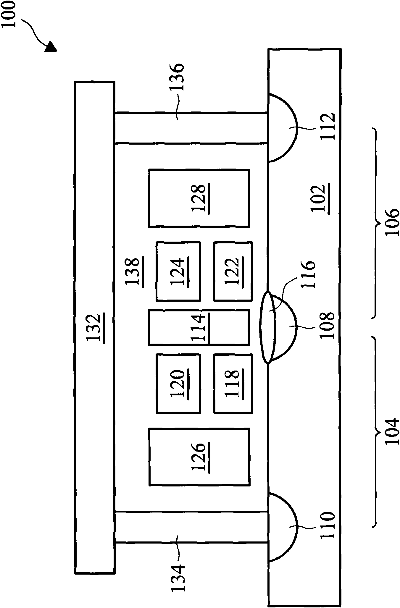
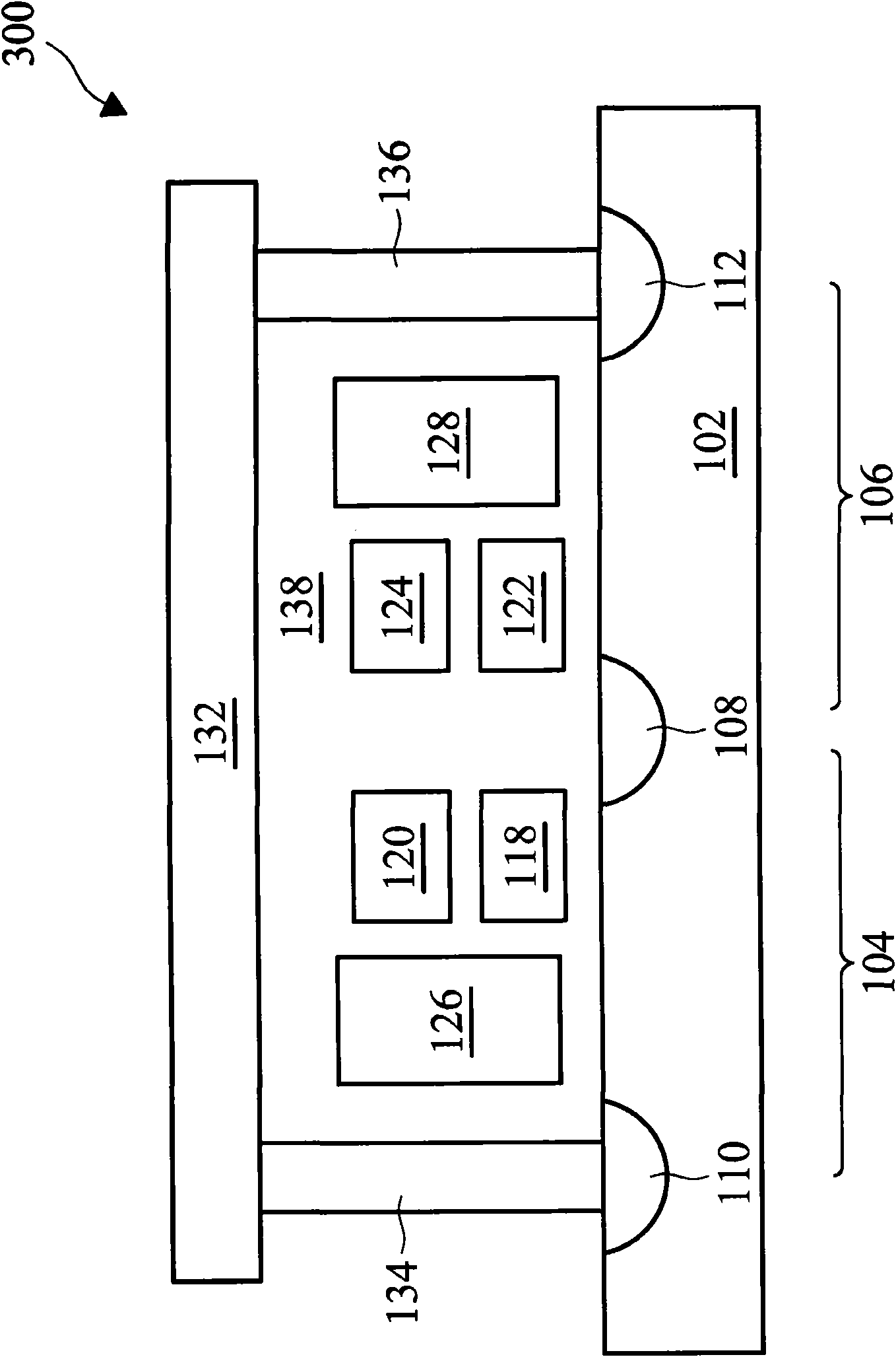
[0042] figure 1 A cross-sectional view of a flash memory structure 100 is shown according to an embodiment of the present invention. The flash memory structure 100 includes a semiconductor substrate 102 . In the disclosed embodiment, the semic...


PUM


Abstract

A method of performing a reading operation to a memory device including a plurality of flash memory cells. The method includes applying a first voltage bias to a control gate of a selected memory cell in the flash memory array and applying a second voltage bias to a word line of the selected memory cell. A control gate of an unselected memory cell in the flash memory array is grounded and a third voltage bias is applied to a word line of the unselected cell to turn off a word line channel of the unselected memory cell. The selected memory cell and unselected memory cell are configured in the memory device and are connected to different word lines. The first voltage bias and the second voltage bias have a same polarity. The third voltage bias and the second voltage bias have opposite polarities.

Description

technical field [0001] This specification mainly deals with the technology of flash memory. Background technique [0002] A conventional flash memory device has a memory array including many memory cells arranged in blocks. Each memory cell has a field effect transistor including a control gate and a floating gate. The floating gate stores charge and the source and drain regions are separated in the body by an oxide. Each memory cell can be electrically charged by injecting electrons into the floating gate. Under an erase operation, charge can be removed from the floating gate by tunneling to the source region or the erase gate. The determination of the data stored in the flash memory unit can be determined according to the presence or absence of charges on the floating gate. [0003] Considering packing density and cost, reducing the size of memory elements is a trend. In general flash memory structures, the need to shorten the word line length due to conflicting facto...

Claims


Application Information

Patent Timeline
Patent Type & Authority Patents(China)
IPC IPC(8): G11C16/06G11C16/26
CPCG11C16/3418G11C16/26G11C16/08
Inventor 谢佳达池育德
Owner TAIWAN SEMICON MFG CO LTD
Features
  • R&D
  • Intellectual Property
  • Life Sciences
  • Materials
  • Tech Scout
  • Unparalleled Data Quality
  • Higher Quality Content
  • 60% Fewer Hallucinations
Learn More