
Method for forming side wall and p-channel metal oxide semiconductor (PMOS) transistor

A transistor and sidewall technology, which is applied in the field of forming sidewalls and PMOS transistors, can solve the problems of increasing stress difference between sidewalls and germanium-silicon, lattice mismatch, sidewall peeling, etc., and achieves the effect of good adhesion

Inactive Publication Date: 2012-05-09
SEMICON MFG INT (SHANGHAI) CORP +1
View PDF6 Cites 0 Cited by
  • Summary
  • Abstract
  • Description
  • Claims
  • Application Information

AI Technical Summary

Problems solved by technology

[0006] However, through transmission electron microscope image analysis, it is found that the side wall formed by the method of the prior art does not have a silicon oxide layer on the contact surface between the silicon germanium region and the side wall, which will cause the stress difference between the side wall and the silicon germanium to change. Large, lattice matching mismatch, so that the sidewall is easy to peel off from the silicon substrate, thus affecting the performance of the device

Method used


Image

  • Method for forming side wall and p-channel metal oxide semiconductor (PMOS) transistor
  • Method for forming side wall and p-channel metal oxide semiconductor (PMOS) transistor
  • Method for forming side wall and p-channel metal oxide semiconductor (PMOS) transistor

Examples


Embodiment Construction

[0039] There is no silicon oxide layer on the contact surface between the silicon germanium region and the side wall of the sidewall spacer formed by the method of the prior art, which causes the stress difference between the sidewall and the silicon germanium region to become larger, the lattice matching is out of adjustment, and the sidewall It is easy to peel off from the silicon substrate, thereby affecting the performance of the device. The inventors have studied hard and found the following reasons: if germanium ion implantation is used to form silicon germanium, when silicon germanium is formed, the surface of the silicon germanium region is damaged by the bombardment of germanium ions; when silicon germanium epitaxial growth is used to form silicon germanium , The adhesion between the surface of the silicon germanium area and silicon oxide is not good. After the silicon germanium region is formed in the silicon substrate, when the silicon germanium region is ion-implant...


PUM


Abstract

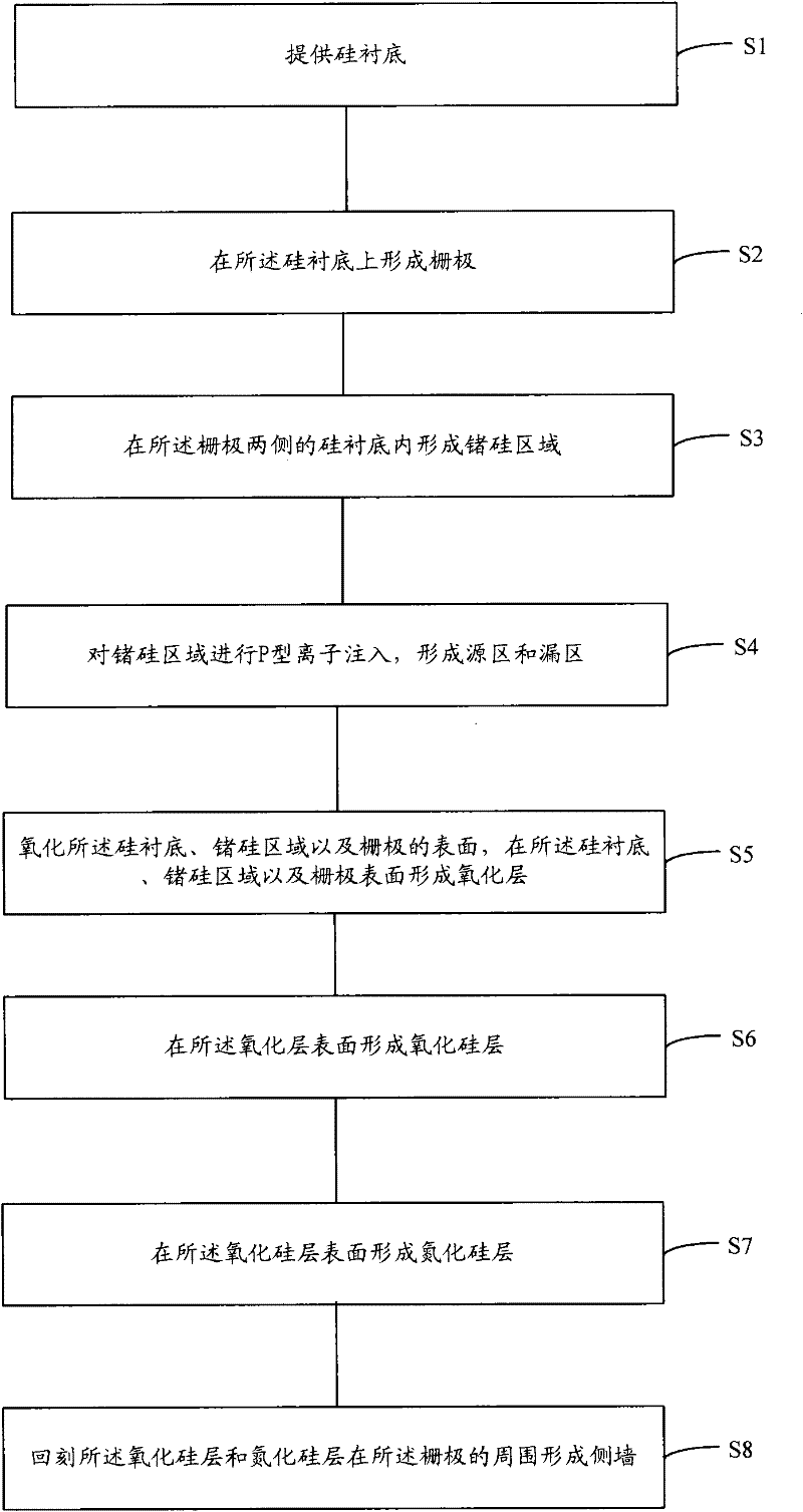
The invention relates to a method for forming a side wall and a p-channel metal oxide semiconductor (PMOS) transistor. The method for forming the side wall comprises the following steps that: a silicon substrate is provided, a grid is formed on the silicon substrate, and a germanium-silicon region is formed inside the silicon substrate at two sides of the silicon grid; the silicon substrate, the germanium-silicon region and the surface of the grid are oxidized so as to form an oxidized layer respectively on the silicon substrate, the germanium-silicon region and the surface of the grid; a silicon oxide layer is formed on the surface of the oxidized layer; a silicon nitride layer is formed on the surface of the silicon oxide layer; and the oxidized layer, the silicon oxide layer and the silicon nitride layer are etched to form a side wall on the periphery of the grid. Due to the adoption of the method, the problem that the side wall is easily separated from the silicon substrate because of no silicon oxide layer on the germanium-silicon region can be solved.

Description

Technical field [0001] The present invention relates to the field of semiconductor technology, in particular to a method for forming sidewalls and PMOS transistors. Background technique [0002] As we all know, mechanical stress can change the energy gap and carrier mobility of silicon materials. Recently, mechanical stress has played an increasingly important role in affecting the performance of MOSFETs. If the stress can be appropriately controlled and the mobility of carriers (electrons in n-channel transistors and holes in p-channel transistors) can be increased, the drive current can be increased, and thus the stress can greatly improve the performance of the transistor. [0003] The stress liner technology forms a tensile stress liner on the NMOS transistor and a compressive stress liner on the PMOS transistor, thereby increasing the driving current of the PMOS transistor and the NMOS transistor, and improving The response speed of the circuit. According to research, integr...

Claims


Application Information

Patent Timeline
Patent Type & Authority Applications(China)
IPC IPC(8): H01L21/311H01L21/31H01L21/336
Inventor 张彬鲍宇任万春
Owner SEMICON MFG INT (SHANGHAI) CORP
Learn More