
Memory cell of phase change random access memory

A technology for accessing memories and memory cells, applied in electrical components, semiconductor devices, electro-solid devices, etc., can solve problems such as reducing the RESET current of phase-change random access memory, reduce the RESET current, improve performance, and reduce power generation. Effects of heat and power consumption

Active Publication Date: 2014-06-25
SEMICON MFG INT (SHANGHAI) CORP +1
View PDF4 Cites 0 Cited by
  • Summary
  • Abstract
  • Description
  • Claims
  • Application Information

AI Technical Summary

Problems solved by technology

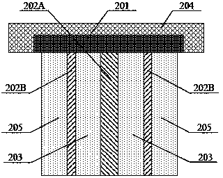
[0008] In order to solve the problem that the prior art cannot effectively and economically reduce the RESET current of the phase change random access memory, the present invention provides a storage unit of the phase change random access memory, the storage unit includes a phase change material layer and a columnar Coaxial electrode; the columnar coaxial electrode includes a first electrode located at the axis position of the columnar coaxial electrode, a second electrode nested outside the first electrode and coaxial with the first electrode, and filling the first insulating layer between the first electrode and the second electrode; the phase change material layer is connected to the same side of the first electrode and the second electrode

Method used


Image

  • Memory cell of phase change random access memory
  • Memory cell of phase change random access memory
  • Memory cell of phase change random access memory

Examples


Embodiment Construction

[0029] In the following description, numerous specific details are given in order to provide a more thorough understanding of the present invention. It will be apparent, however, to one skilled in the art that the present invention may be practiced without one or more of these details. In other examples, some technical features known in the art are not described in order to avoid confusion with the present invention.

[0030] In order to thoroughly understand the present invention, a detailed structure will be presented in the following description to illustrate how the present invention can effectively and economically reduce the RESET current of the phase change random access memory. Obviously, the practice of the invention is not limited to specific details familiar to those skilled in the semiconductor arts. Preferred embodiments of the present invention are described in detail below, however, the present invention may have other embodiments besides these detailed descrip...


PUM


Abstract

The invention discloses a memory cell of a phase change random access memory, wherein the memory cell comprises a phase change material layer and a columnar coaxial electrode, wherein the columnar coaxial electrode comprises a first electrode, a second electrode and a first insulation layer; the first electrode is positioned on the axis position of the columnar coaxial electrode; the second electrode is nested out of the first electrode and is coaxial with the first electrode; the first insulation layer is filled between the first electrode and the second electrode; and the phase change material layer is connected with the same side of the first electrode and the second electrode. The invention also discloses the phase change random access memory which comprises a control circuit, a memory cell layer, a strobe device layer and a substrate. According to the memory cell of the phase change random access memory and the phase change random access memory provided by the invention, the heat productivity and power consumption of the phase change random access memory and a circuit using the phase change random access memory can be lowered effectively, and performances of the phase change random access memory and the circuit using the phase change random access memory are improved economically.

Description

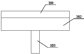
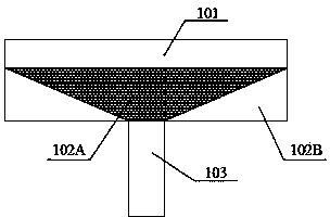
technical field [0001] The invention relates to the technical field of semiconductors, in particular to a storage unit of a phase change random access memory (PCRAM). Background technique [0002] Phase-change materials (such as Ge-Sb-Te phase-change materials) change their phase state into crystalline and amorphous states through local heating caused by electric pulses. Phase-change random access memory uses this characteristic to store binary information Semiconductor device. Phase-change random access memory is a memory based on resistance. Through the conversion of phase-change materials between crystalline and amorphous states, the resistance characteristics of low resistance and high resistance are correspondingly presented to store binary information. In a phase change random access memory, a memory cell that stores binary information includes a phase change material layer and electrodes. [0003] Figure 1A It is a structural diagram of a memory cell of a phase cha...

Claims


Application Information

Patent Timeline
Patent Type & Authority Patents(China)
IPC IPC(8): H01L45/00H01L27/24
Inventor 吴关平徐成刘燕
Owner SEMICON MFG INT (SHANGHAI) CORP
Learn More