Hafnium-oxynitride-based low-power consumption resistive random access memory and preparation method for same

A technology of resistive memory and hafnium oxynitride, which is applied in the field of microelectronics, can solve the problems of large reset current and power consumption, and achieve the effects of reducing reset current, reducing power consumption and increasing resistance

Active Publication Date: 2015-02-18
TIANJIN UNIVERSITY OF TECHNOLOGY
View PDF6 Cites 0 Cited by
  • Summary
  • Abstract
  • Description
  • Claims
  • Application Information

AI Technical Summary

Problems solved by technology

[0006] According to the above literature, using a single layer of metal oxide as the resistive variable layer has the problem of large reset current and large power consumption.

Method used


Image

  • Hafnium-oxynitride-based low-power consumption resistive random access memory and preparation method for same
  • Hafnium-oxynitride-based low-power consumption resistive random access memory and preparation method for same
  • Hafnium-oxynitride-based low-power consumption resistive random access memory and preparation method for same

Examples


Embodiment 1

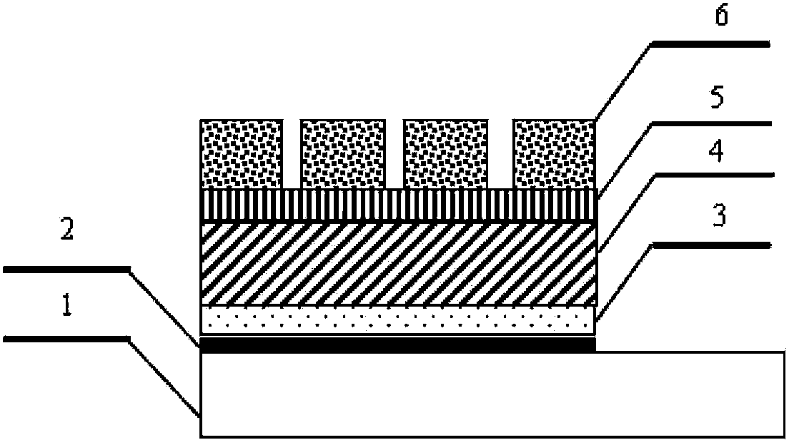
[0030] A low-power resistive memory based on hafnium oxynitride, its structure is as follows figure 1 As shown, by silicon oxide substrate 1, 5nm thick Ti adhesion layer 2, 100nm thick Pt as the lower electrode 3, 50nm thick hafnium oxynitride 4, 10nm thick metal hafnium thin film 5 and 100nm thick Pt as The upper electrode 6 constitutes.

[0031] The preparation method of the resistive memory, the steps are as follows:

[0032] 1) The silicon oxide wafer is used as the substrate, and the silicon oxide wafer is SiO on the surface after the silicon is oxidized. 2 Oxide silicon wafer;

[0033] 2) Prepare a 5nm thick Ti adhesion layer on a silicon oxide wafer by ion beam sputtering;

[0034] 3) Deposit 100nm thick Pt as the bottom electrode by electron beam evaporation process;

[0035] 4) A 50nm-thick hafnium oxynitride film was prepared on the lower electrode by reactive magnetron sputtering. The sputtering process conditions were: metal hafnium target sputtering target wit...

Embodiment 2

[0042] A low-power resistive memory based on hafnium oxynitride and its preparation method, its structure is as follows figure 1 As shown, a silicon oxide substrate 1, a 5nm thick Ti adhesion layer 2, a 100nm thick TiN as the lower electrode 3, a 50nm thick hafnium oxynitride 4, a 10nm thick metal hafnium thin film 5 and a 100nm thick TiN It is formed as the upper electrode 6 .

[0043] The preparation method of the resistive memory, the steps are as follows:

[0044] 1) The silicon oxide wafer is used as the substrate, and the silicon oxide wafer is SiO on the surface after the silicon is oxidized. 2 Oxide silicon wafer;

[0045] 2) Prepare a 10nm-thick Ti adhesion layer on the silicon oxide wafer by ion beam sputtering;

[0046] 3) A 100nm-thick TiN lower electrode was deposited on the Ti adhesion layer by DC reactive magnetron sputtering. The sputtering process: the target intercept was 6.5cm, and the background vacuum was 5×10 -4 Pa, the working pressure is 0.5Pa, the sp...


PUM


Abstract

The invention discloses a hafnium-oxynitride-based low-power consumption resistive random access memory and a preparation method for the same. The hafnium-oxynitride-based low-power consumption resistive random access memory consists of a silicon oxide chip substrate, a Ti adhesion layer, a lower electrode, a resistance variable layer and an upper electrode, which are sequentially stacked, wherein the resistance variable layer is in a laminated structure of a hafnium oxynitride thin film and a metal hafnium thin film. The preparation method comprises the steps of sequentially preparing each layer of thin film in a magnetron sputtering way, an ion beam sputtering way or an electron beam evaporation way respectively. The hafnium-oxynitride-based low-power consumption resistive random access memory and the preparation method for the same have the advantages that the laminated structure of the hafnium oxynitride thin film and the metal hafnium thin film is adopted as the resistance variable layer, so that the formation of a transition oxygen vacancy is inhibited by nitrogen in hafnium oxynitride in a set process, low-resistance state resistance is improved, the reset current of the memory is reduced, and the power consumption of the memory is lowered.

Description

technical field [0001] The invention belongs to the technical field of microelectronics, and in particular relates to a low-power resistive memory based on hafnium oxynitride and a preparation method thereof. technical background [0002] Resistive variable memory (RRAM) is composed of a simple sandwich structure (MIM) metal-resistive layer-metal. Due to its fast switching speed, large integration density, long retention time, and the potential for multi-value storage, In recent years, it has been deeply explored by a large number of researchers. Therefore, the resistive memory is likely to replace the traditional flash memory with a floating gate structure and become a new generation of non-volatile memory. [0003] Resistive memory devices represent "0" with high resistance, "1" with low resistance, and store data through high and low resistance values. The transition from a high resistance state to a low resistance state is called a set process, and there is usually a c...

Claims


Application Information

Patent Timeline
Patent Type & Authority Patents(China)
IPC IPC(8): H01L45/00G11C13/00
Inventor 张楷亮孙阔王芳陆涛孙文翔韦晓莹王宝林冯玉林赵金石
Owner TIANJIN UNIVERSITY OF TECHNOLOGY
Why Eureka
Try Eureka