Phase change memory and method of fabricating the same

a phase change memory and manufacturing method technology, applied in the field of phase change memory, can solve the problems of increasing surface hole defect, increasing temperature rise and fall, and increasing current requirements, so as to reduce manufacturing costs, improve manufacturing yield, and simplify the manufacturing process of phase change memory.

Active Publication Date: 2020-10-20
JIANGSU ADVANCED MEMORY TECH CO LTD +1
View PDF6 Cites 0 Cited by
  • Summary
  • Abstract
  • Description
  • Claims
  • Application Information

AI Technical Summary

Benefits of technology

[0023]As can be seen from the above embodiments, the present disclosure provides a phase change memory. In the manufacturing process of the phase change memory, the annular heater and the annular phase change layer do not need to be precisely aligned, and the contact area between the annular heater and the annular phase change layer can be reduced by misaligning the two. That is, the present disclosure simplifies the manufacturing process of the phase change memory, reduces the manufacturing cost, and improves the manufacturing yield. In addition, the contact area between the heater and the phase change layer of the phase change memory of the present disclosure is very small, so that the phase change memory has an extremely low reset current thus to effectively solve the problems described in the prior art.

Problems solved by technology

The heater of the conventional phase change memory element has a large contact area with a memory element coupled thereto, which will increase surface hole defect, and rates of the temperature rise and fall are also slow (the conversion between high resistance and low resistance value is not fast enough), and an amount of current required is also large.
In addition, the process of manufacturing a heater having a small contact area using conventional technology requires a precise alignment mechanism, which results in a complicated process and is difficult to control, and relatively increases the manufacturing cost of the phase change memory.

Method used


Image

  • Phase change memory and method of fabricating the same
  • Phase change memory and method of fabricating the same
  • Phase change memory and method of fabricating the same

Examples


Embodiment Construction

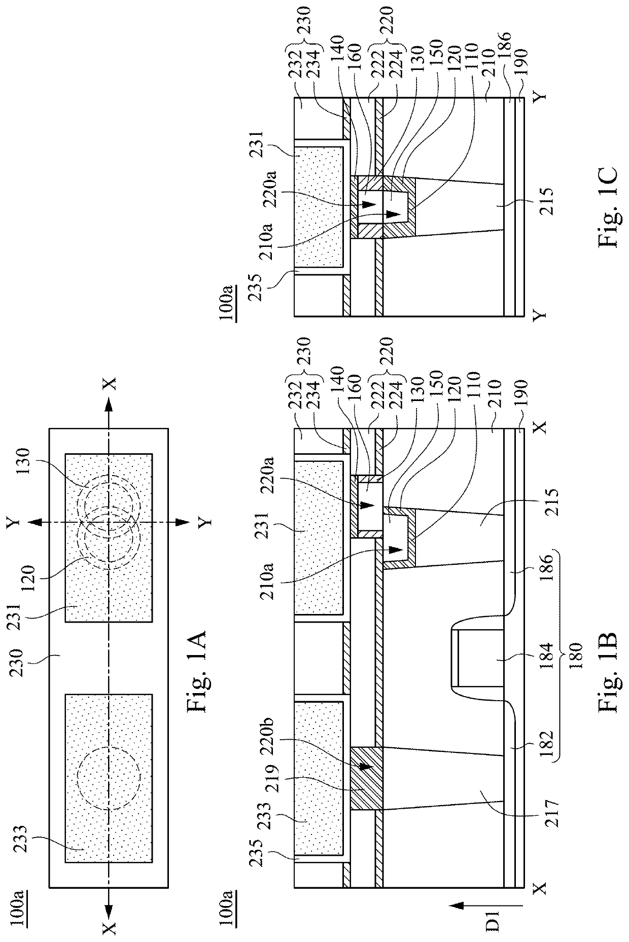
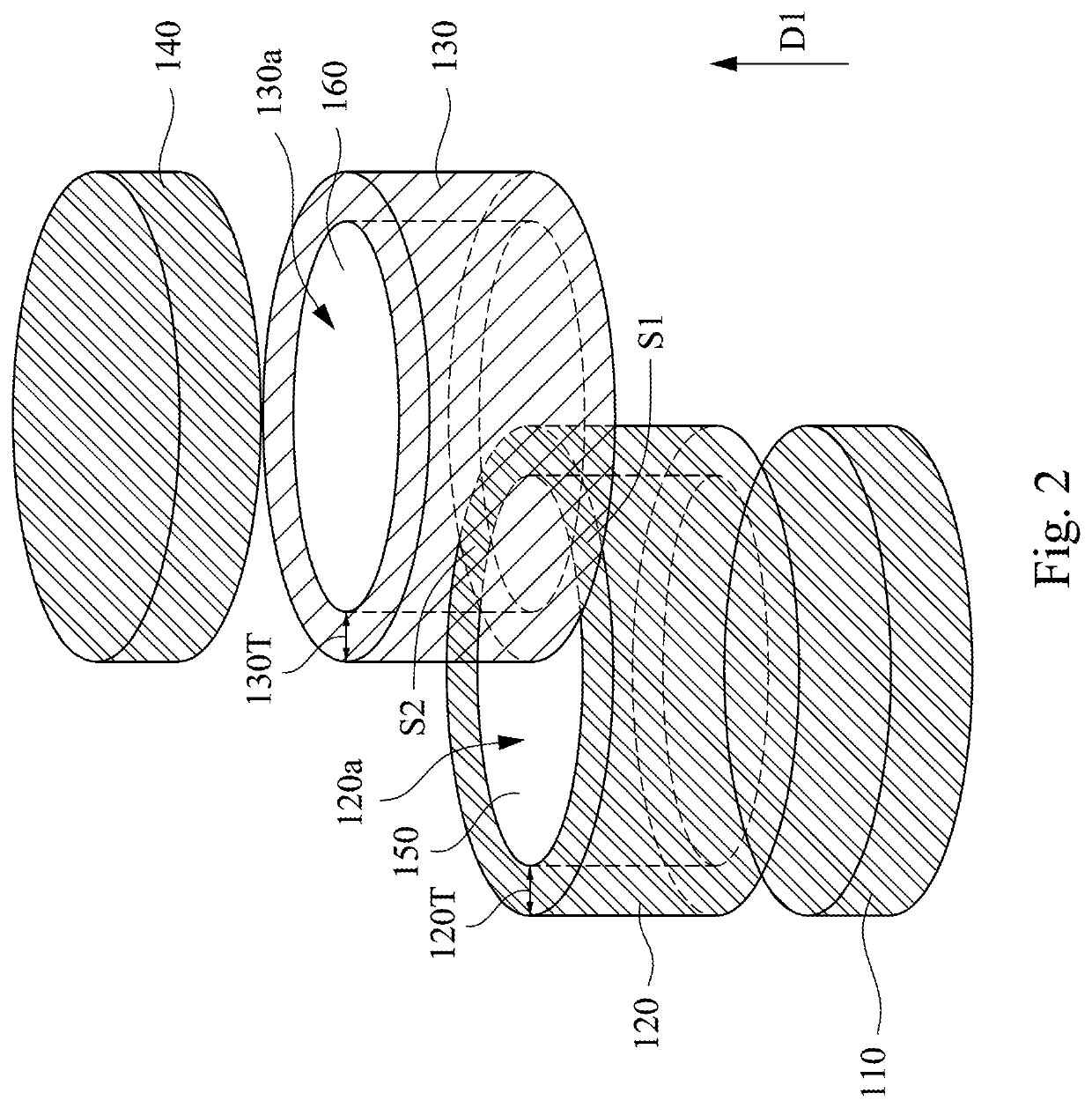
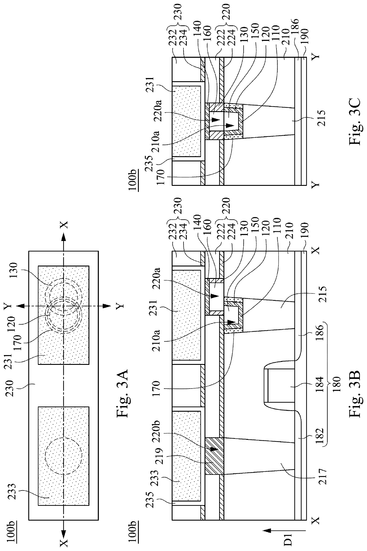
[0041]The following disclosure provides many different embodiments or examples for implementing different features of the subject matter provided. Specific examples of components and arrangements are described below to simplify the disclosure. These are merely examples and are not intended to limit the disclosure. For example, forming a first feature over a second feature or on a second feature in a subsequent description may include an embodiment of forming the first feature and the second feature that are in direct contact, and may also include an embodiment of forming an additional feature between the first and second features such that the first and second features are not in direct contact. In addition, in each example of the present disclosure, element reference numerals and / or letters may be repeated. This repetition is for the purpose of simplification and clarity, and is not intended to indicate the relationship between the various embodiments and / or constructions discussed...


PUM

PropertyMeasurementUnit
thicknessaaaaaaaaaa
thicknessaaaaaaaaaa
thicknessaaaaaaaaaa

Abstract

A phase change memory and a method of fabricating the same are provided. The phase change memory includes a lower electrode, an annular heater, an annular phase change layer, and an upper electrode. The annular heater is disposed over the lower electrode. The annular phase change layer is disposed over the annular heater, and the annular phase change layer and the annular heater are misaligned in a normal direction of the lower electrode. The upper electrode is disposed over the annular phase change layer. The present disclosure simplifies the manufacturing process of the phase change memory, reduces the manufacturing cost, and improves the manufacturing yield. In addition, a contact surface between the heater and the phase change layer of the phase change memory of the present disclosure is very small, so that the phase change memory has an extremely low reset current.

Description

CROSS-REFERENCE TO RELATED APPLICATION[0001]This application claims priority to China Application Serial Number 201910202172.X, filed Mar. 18, 2019, which is herein incorporated by reference.BACKGROUNDField of Invention[0002]The present disclosure relates to a phase change memory and a method of fabricating the phase change memory.Description of Related Art[0003]Electronic products, such as cell phones, tablets, and digital cameras, often have memory elements that store data. The conventional memory element can store data through a storage node on the memory cell. Among them, the phase change memory utilizes the electrical resistance state (e.g., high resistance and low resistance) of the memory element to store data. The memory element can have a material that can be switched between different phase states (e.g., a crystalline phase and an amorphous phase). The different phase states cause the memory cell to have electrical resistance states of different electrical resistance value...

Claims


Application Information

Patent Timeline
Patent Type & Authority Patents(United States)
IPC IPC(8): H01L45/00H01L27/24
CPCH01L45/126H01L27/2436H01L45/1233H01L45/06H01L45/1683H01L45/148H01L45/144H10B63/30H10N70/8413H10N70/8613H10N70/231H10N70/826H10N70/8828H10N70/066H10N70/884
Inventor CHENG, SHENG-HUNGCHANG, MING-FENGYANG, TZU-HAO
Owner JIANGSU ADVANCED MEMORY TECH CO LTD
Why Eureka
Try Eureka