Shift register circuit, display device provided with same, and shift register circuit driving method

A shift register, potential technology, used in static memory, digital memory information, instruments, etc.

Inactive Publication Date: 2012-05-16
SHARP KK
View PDF5 Cites 16 Cited by
  • Summary
  • Abstract
  • Description
  • Claims
  • Application Information

AI Technical Summary

Problems solved by technology

Therefore, the gate bus line connected to the output terminal 89 of the bistable circuit becomes a non-selected state.

Method used


Image

  • Shift register circuit, display device provided with same, and shift register circuit driving method
  • Shift register circuit, display device provided with same, and shift register circuit driving method
  • Shift register circuit, display device provided with same, and shift register circuit driving method

Examples


Embodiment Construction

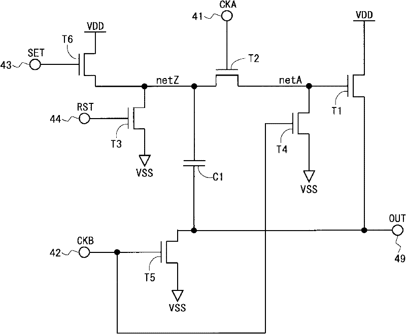
[0130] One embodiment of the present invention will be described below with reference to the drawings. Wherein, in the following description, the gate terminal (gate electrode) of the thin film transistor corresponds to the first electrode, the drain terminal (drain electrode) corresponds to the second electrode, and the source terminal (source electrode) corresponds to the second electrode. Three electrodes.

[0131]

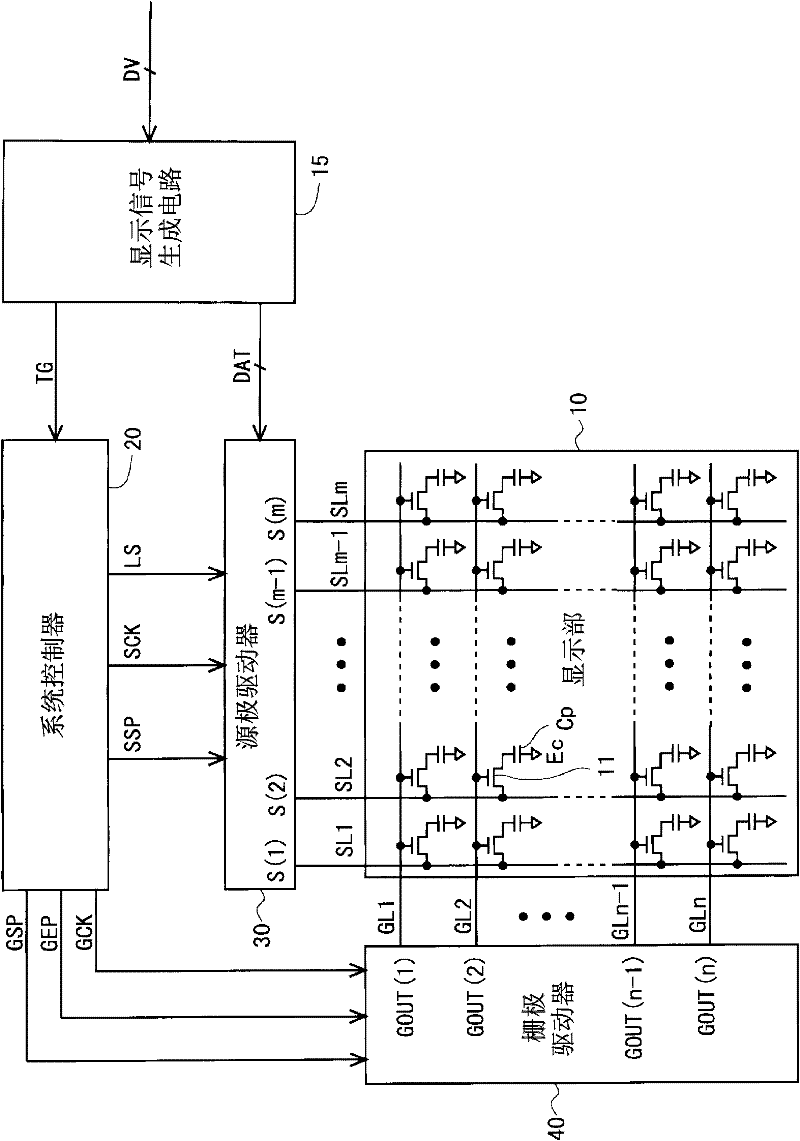
[0132] figure 2 It is a block diagram showing the overall configuration of an active matrix liquid crystal display device according to one embodiment of the present invention. Such as figure 2 As shown, the liquid crystal display device includes a display unit 10 , a display signal generating circuit 15 , a system controller 20 , a source driver (video signal line driving circuit) 30 and a gate driver (scanning signal line driving circuit) 40 .

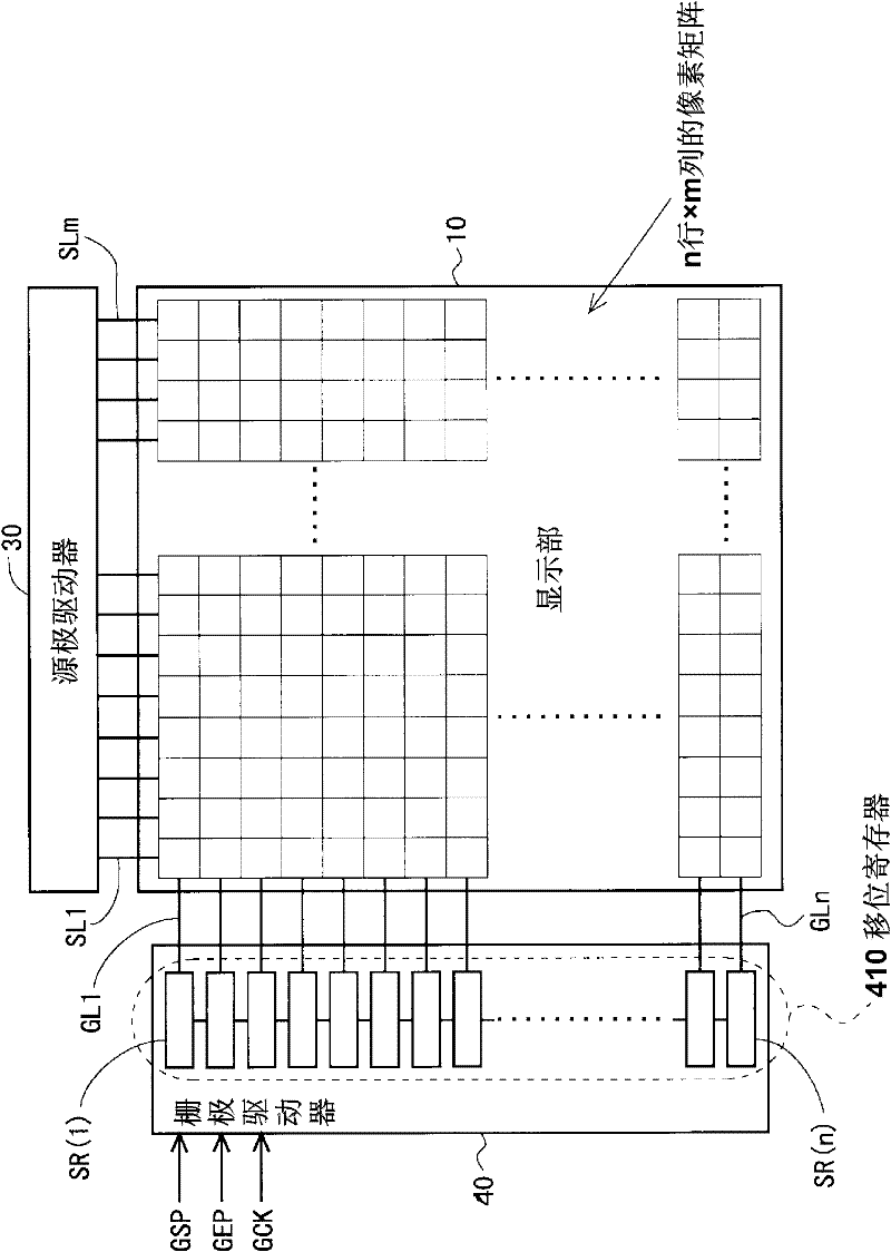
[0133] The display unit 10 includes a plurality (m) of source bus lines (video signal lines) SL1 to SLm, a pl...


PUM


Abstract

Disclosed is a display device capable of inhibiting degradation of visual quality that has been caused by crosstalk, without causing an increase in frame size or an increase in power consumption. Each bistable circuit is provided with an output terminal (49) that outputs a state signal; a thin-film transistor (T1), the drain terminal of which is given a high-level potential (VDD), and the source terminal of which is connected to the output terminal (49); a thin-film transistor (T2), the source terminal of which is connected to an area netA that is connected to the gate terminal of the thin-film transistor (T1), and the gate terminal of which is given a clock (CKA); a thin-film transistor (T6) for increasing a potential of an area netZ that is connected to the drain terminal of the thin-film transistor (T2); and thin-film transistors (T4, T5, T3) for lowering each of the potentials of netA, netC, and the output terminal (49). A channel area of the thin-film transistor (T1) is made to be larger than a channel area of the thin-film transistor (T2).

Description

technical field [0001] The present invention relates to a shift register provided in a driving circuit of an active matrix type display device and a driving method thereof. Background technique [0002] Known in the prior art is an active matrix display device in which a plurality of gate bus lines (scanning signal lines) and a plurality of source bus lines (video signal lines) are arranged in a grid pattern, and these plurality of gate bus lines A plurality of pixel forming portions are arranged in a matrix to correspond to intersection points of the plurality of source bus lines. Each pixel forming part includes a TFT (thin film transistor: Thin Film Transistor) as a switching element and a pixel capacitor for holding a pixel value. The sub is connected to the source bus through this crosspoint. The active matrix display device further includes a gate driver (scanning signal line driver circuit) for driving the plurality of gate bus lines, and a source driver (video sign...

Claims


Application Information

Patent Timeline
Patent Type & Authority Applications(China)
IPC IPC(8): G11C19/28G09G3/20G09G3/36G11C19/00
CPCG09G3/3685G11C19/28G09G2310/0286G09G3/3275G09G2320/0209G11C19/184
Inventor 大桥诚二
Owner SHARP KK
Why Eureka
Try Eureka