Preparation method of transmission electron microscope (TEM) sample

A sample and sample technology, applied in the field of TEM sample preparation, can solve the problems of no way to use TEM, damage in the thickness direction, amorphization, etc.

Active Publication Date: 2012-05-23
SEMICON MFG INT (SHANGHAI) CORP +1
View PDF7 Cites 13 Cited by
  • Summary
  • Abstract
  • Description
  • Claims
  • Application Information

AI Technical Summary

Problems solved by technology

[0009] However, in the above-mentioned existing preparation method, in the step of ion thinning, the ion beam with high precision is used to aim at the pattern to be detected to bombard the thinned sample. Ga ion beam is commonly used in the prior art, but this thinning The method can only be thinned to about 100nm, because there is damage in the thickness direction of the sample, and if it continues to be thinned, it will lead to amorphization in the thickness direction of the sample, so there is no way to use TEM to observe the original morphology of the sample

Method used


Image

  • Preparation method of transmission electron microscope (TEM) sample
  • Preparation method of transmission electron microscope (TEM) sample
  • Preparation method of transmission electron microscope (TEM) sample

Examples


preparation example Construction

[0034] Figure 5 It is a flowchart of the preparation method of the TEM sample of the present invention. Such as Figure 5 Shown, the preparation method of TEM sample of the present invention comprises steps:

[0035] S10, providing a detection sample, the detection sample has a pattern to be detected;

[0036] S20, cutting out a sample from the test sample, the sample including a pattern to be detected;

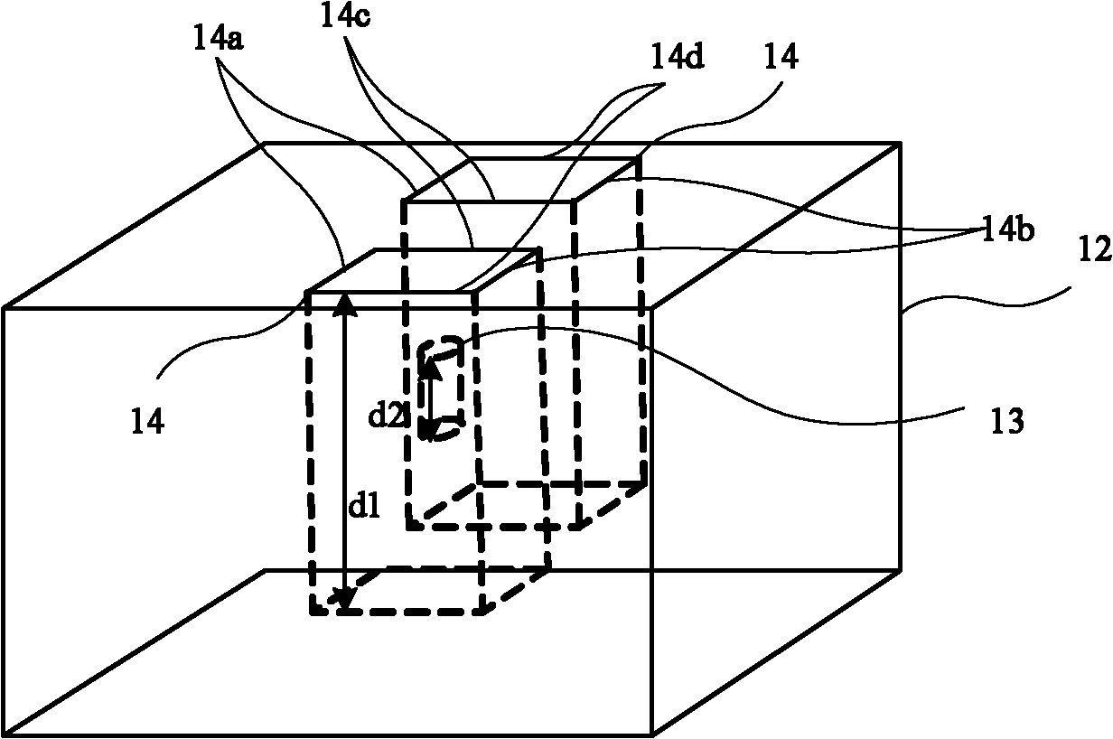
[0037] S30, thinning the sample from two opposite cutting surfaces of the sample, and sticking a fixing ring on one of the thinned cutting surfaces;

[0038] S50, clamping the fixing ring, using Ga ion beams to bombard the regions on both sides of the pattern to be detected on the side of the sample having the device layer, so as to form pits on both sides of the pattern to be detected;

[0039] S60, clamping the fixing ring, bombarding the thinned cutting surface with an Ar ion beam, and continuing to thin the area where the pattern to be detected is located.


PUM

PropertyMeasurementUnit
thicknessaaaaaaaaaa
thicknessaaaaaaaaaa
thicknessaaaaaaaaaa

Abstract

The invention provides a preparation method of a TEM sample. The preparation method comprises the following steps of 1, preparing a sample needing to be detected, wherein the sample is provided with a pattern needing to be detected, 2, cutting the sample to obtain a sample wafer, wherein the sample wafer comprises the pattern needing to be detected, 3, thinning the sample wafer from two opposite cut surfaces, and pasting a fixing ring on one of the thinned cut surfaces, 4, clamping the fixing ring, and through a Ga ion beam, bombarding areas which belong to one sample wafer surface provided with the pattern needing to be detected and are located at two sides of the pattern needing to be detected, so that the two sides of the pattern needing to be detected form pits, 5, clamping the fixing ring, and bombarding the thinned cut surfaces by an Ar ion beam, and 6, sequentially thinning an area comprising the pattern needing to be detected. The preparation method provided by the invention improves efficiency and reduces a cost.

Description

technical field [0001] The invention relates to the technical field of semiconductor manufacturing, in particular to the field of sample preparation methods for TEM (Transmission Electron Microscope). Background technique [0002] In the semiconductor manufacturing industry, there are a variety of inspection equipment, among which EM is an important tool for inspecting the morphology, size and characteristics of the thin films that make up the device. Commonly used EMs include TEM (Transmission Electron Microscope) and SEM (Scanning Electron Microscope). The working principle of TEM is to thin the sample to be tested by cutting, grinding, ion thinning, etc., and then put it into the TEM observation room, irradiate the sample with a high-voltage accelerated electron beam, enlarge the shape of the sample, and project it on the screen. One of the outstanding advantages of TEM is that it has a high resolution and can observe the shape and size of extremely thin films. [0003]...

Claims


Application Information

Patent Timeline
Patent Type & Authority Applications(China)
IPC IPC(8): G01N1/28
Inventor 李明段淑卿芮志贤赵燕丽陈祯祥
Owner SEMICON MFG INT (SHANGHAI) CORP
Why Eureka
Try Eureka