Process for producing SiC single crystal

A manufacturing method and single crystal technology, applied in the direction of single crystal growth, single crystal growth, chemical instruments and methods, etc., can solve problems such as helplessness

Active Publication Date: 2012-05-23
TOYOTA JIDOSHA KK
View PDF8 Cites 13 Cited by
  • Summary
  • Abstract
  • Description
  • Claims
  • Application Information

AI Technical Summary

Problems solved by technology

This is also a technique to control the temperature distribution in the crystal in the sublimation method, which is different from the melt method, and does not contribute at all to the reduction of defects caused by seed contact in the growth of SiC single crystals using the melt method

Method used


Image

  • Process for producing SiC single crystal
  • Process for producing SiC single crystal
  • Process for producing SiC single crystal

Examples


Embodiment

[0048] Growth of SiC single crystal was carried out in the following procedure.

[0049] Basic Crystal Growth Process

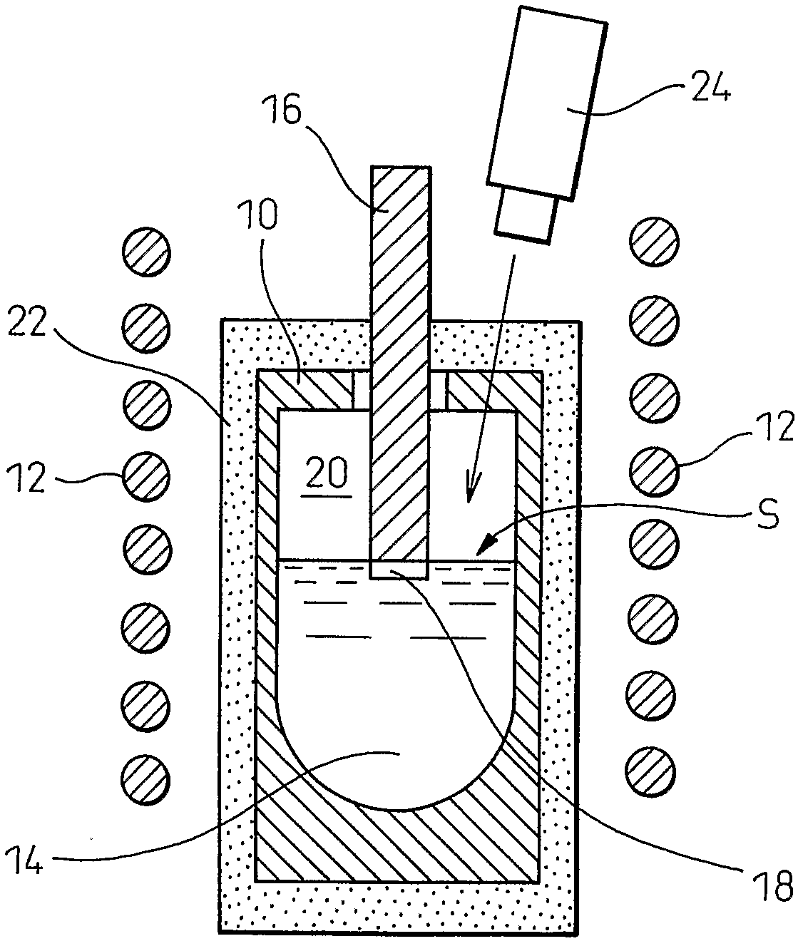
[0050] · Growth preparation (refer to figure 1 )

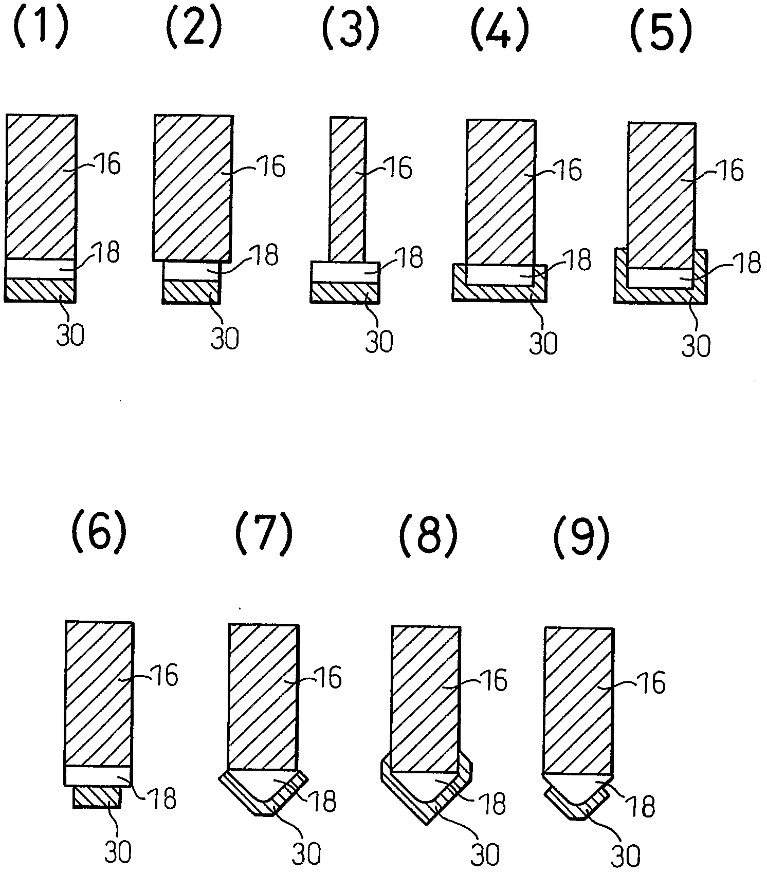
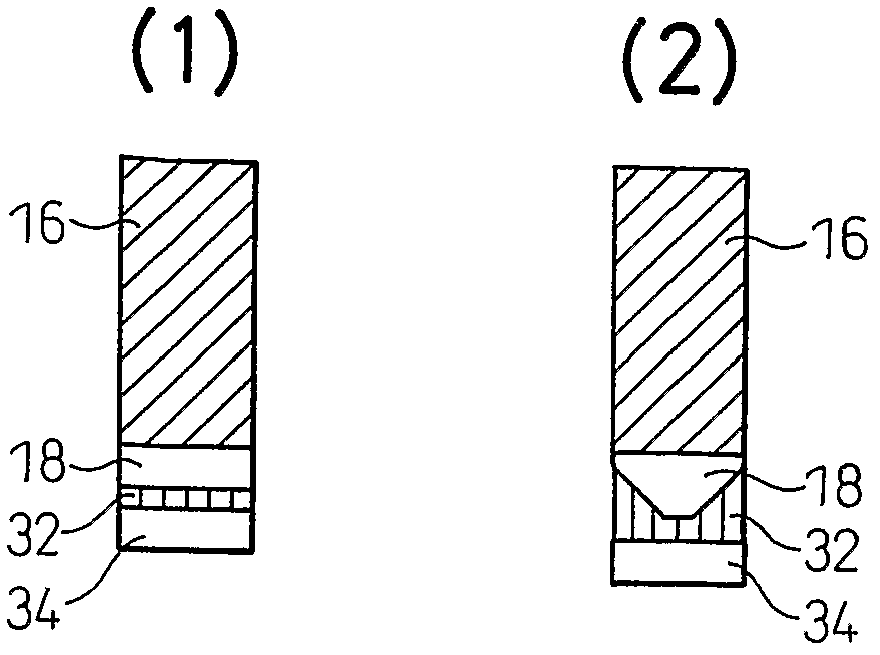
[0051] (1) The 4H-SiC seed crystal 18 is joined to the supporting shaft 16 made of graphite.

[0052] (2) Putting raw materials into the graphite crucible 10 .

[0053] (3) Put them as figure 1 constituted as shown.

[0054] (4) Ar20 at atmospheric pressure is introduced.

[0055] (5) Raise the temperature to the desired temperature.

[0056] ·Seed contact

[0057] (1) When the temperature of the melt 14 reaches a sufficient temperature, the support shaft 16 is lowered.

[0058] (2) After the seed crystal 18 comes into contact with the melt 14, the shaft 16 is lowered to a desired depth (*), and then the shaft is stopped. (*: In this embodiment, the seed crystal 18 stops at the position where it touches the liquid surface of the melt 14. In general, the seed crystal 18 sometimes sinks into the melt 1...

Embodiment 1

[0069] According to the present invention, the seed crystal contact is performed without temperature maintenance during the temperature increase.

[0070] The temperature of the melt was raised, and when the temperature reached 1900° C., seed crystal contact was performed immediately without temperature maintenance, the temperature was raised to 1950° C., and growth was performed at this temperature for 1 hour. A SiC single crystal with a thickness of about 60 μm can be obtained. The crystal was subjected to molten KOH etching, and the density of etch pits was 3×10 3 cm -2 . This corresponds to a seed defect density level of 10 3 cm -2 equal.

[0071] Compared with Comparative Example 2, the thickness of the obtained crystal was about 60 μm thinner. Also, although the seed contact was performed at the same temperature as in Comparative Example 2, the dislocation density was 2 orders of magnitude less. Thus, according to the present invention, by performing the seed crys...

Embodiment 2

[0081] Growth was performed using a solution in which 40 atomic % of Cr was added to Si. After raising the temperature to the growth temperature of 1950° C., seed contacting is carried out according to the invention without temperature holding. Growth was performed for 1 hour. The resulting SiC single crystal has an etch pit density of 7×10 4 cm -2 .


PUM


Abstract

Disclosed is a process for producing an SiC single crystal by a solution method. The process can prevent defects attributable to seed touch in which seed crystals are brought into contact with a solution to grow SiC single crystals with reduced defect density. The process comprises bringing SiC seed crystals into contact with a melt containing Si within a graphite crucible to grow SiC single crystals on the SiC seed crystals and is characterized in that the SiC seed crystals are brought into contact with the melt in such a state that C is unsaturated.

Description

technical field [0001] The present invention relates to a method for producing a SiC single crystal using a melt method. Background technique [0002] Since SiC has a larger energy bandgap than Si, various techniques for producing a high-quality SiC single crystal suitable as a semiconductor material or the like have been proposed. Various methods have been tried so far as methods for producing SiC single crystals, but the sublimation method and the melt method are most commonly used at present. Although the sublimation method has a fast growth rate, it has the disadvantages of easily producing defects such as micro-shrinkage cavities and / or crystal polymorphic transformation. In contrast, the melt method, which has a relatively slow growth rate but does not have these disadvantages, is considered to be very promising. hope. [0003] In the method for producing a SiC single crystal by the melt method, a temperature gradient is maintained in the Si melt in the graphite cruc...

Claims


Application Information

Patent Timeline
Patent Type & Authority Applications(China)
IPC IPC(8): C30B29/36
CPCC30B19/04C30B29/36C30B19/02C30B15/14C30B17/00
Inventor 旦野克典关章宪斋藤广明河合洋一郎
Owner TOYOTA JIDOSHA KK
Why Eureka
Try Eureka