Variable gain amplifier
A gain amplifier and variable technology, applied in amplifiers, amplifier combinations, radio frequency amplifiers, etc., can solve the problem of large deterioration of distortion characteristics, and achieve the effect of suppressing distortion characteristics and reducing power consumption
- Summary
- Abstract
- Description
- Claims
- Application Information
AI Technical Summary
Problems solved by technology
Method used
Image

Examples
no. 1 Embodiment approach
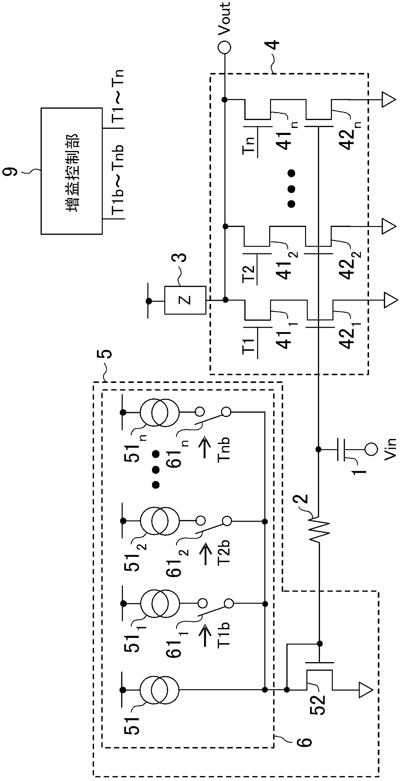
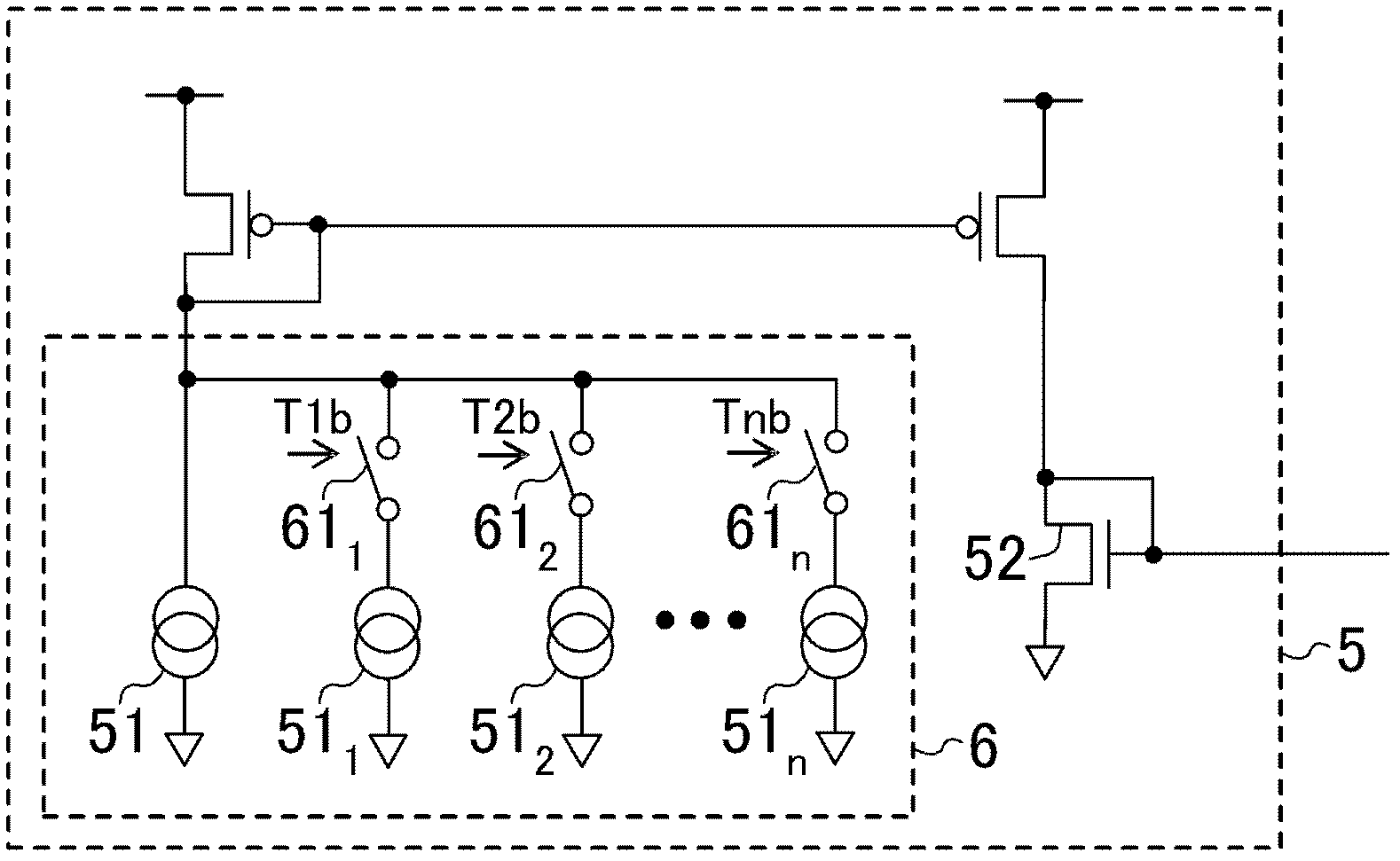
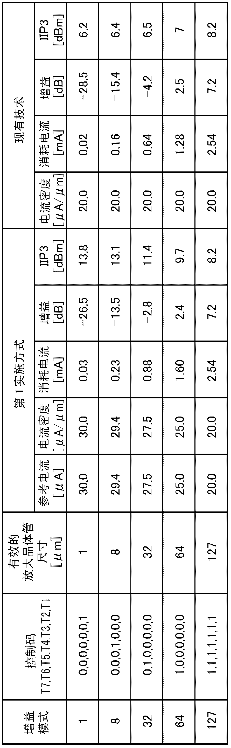
[0063] figure 1 The circuit configuration of the variable gain amplifier according to the first embodiment is shown. The signal Vin is input to the variable amplification unit 4 via the DC blocking capacitor 1, and the signal Vin is converted into a current signal. Thereafter, the current signal is converted into a signal Vout by the load impedance unit 3 . The input of the variable amplifying section 4 is biased by the variable bias voltage supplied from the variable bias voltage generating section 5 via the bias resistor 2 .
[0064] The variable amplifying section 4 is composed of a circuit in which n stages of cascode circuits are connected in parallel, and the cascode circuit is formed by connecting cascode transistors 41 i (1≤i≤n) and amplifier transistor 42 i And constitute. The variable bias generator 5 is composed of a variable current source 6 and a reference transistor 52 . The variable current source 6 consists of a constant current source 51 connected in ser...
no. 2 Embodiment approach
[0071] Figure 5 The circuit configuration of the variable gain amplifier according to the second embodiment is shown. Differences from the first embodiment will be described below.
[0072] The variable bias generator 5 is composed of a constant current source 51 and a variable reference transistor circuit 7 . The variable reference transistor circuit 7 consists of a reference transistor 52 i and switch 71 i The series-connected reference transistor circuit is configured by connecting n-stage circuits in parallel and the reference transistor 52 connected in parallel with the circuits. The reference transistor 52 may also be omitted. By the variable reference transistor circuit 7 and the amplifier transistor 42 i A current mirror circuit is configured to supply a bias current corresponding to the transistor size ratio to the variable amplifying section 4 with respect to the reference current supplied from the constant current source 51 .
[0073] The gain control section...
no. 3 Embodiment approach
[0078] Figure 8 The circuit configuration of the variable gain amplifier according to the third embodiment is shown. Differences from the first embodiment will be described below.
[0079] The variable bias generator 5 is composed of a constant voltage source 53 and a variable voltage dividing circuit 8 . The variable voltage divider circuit 8 consists of a resistor 81 i and switch 82 i The series-connected resistor circuit is configured by connecting n stages of circuits in parallel and resistors 83 connected in series with the circuits. will utilize resistor 81 i The voltage obtained by dividing the voltage supplied from the constant voltage source 53 by the sum resistor 83 is supplied as a variable bias voltage. In addition, the resistor 81 can also be used in the variable voltage divider circuit 8 i All connected in series. At this time, if Figure 9 As shown, as long as the switch 82 controlled by the control signal Si i One end of it can be used as the bias out...
PUM
 Abstract
Description
Claims
Application Information
 - R&D Engineer
- R&D Manager
- IP Professional
- Industry Leading Data Capabilities
- Powerful AI technology
- Patent DNA Extraction
Browse by: Latest US Patents, China's latest patents, Technical Efficacy Thesaurus, Application Domain, Technology Topic.
© 2024 PatSnap. All rights reserved.Legal|Privacy policy|Modern Slavery Act Transparency Statement|Sitemap