

Memory system
A storage system and storage unit technology, applied in the field of storage systems, can solve problems such as data errors, expansion, and write errors
- Summary
- Abstract
- Description
- Claims
- Application Information
AI Technical Summary
Problems solved by technology
Method used
Image

Examples
no. 1 Embodiment approach
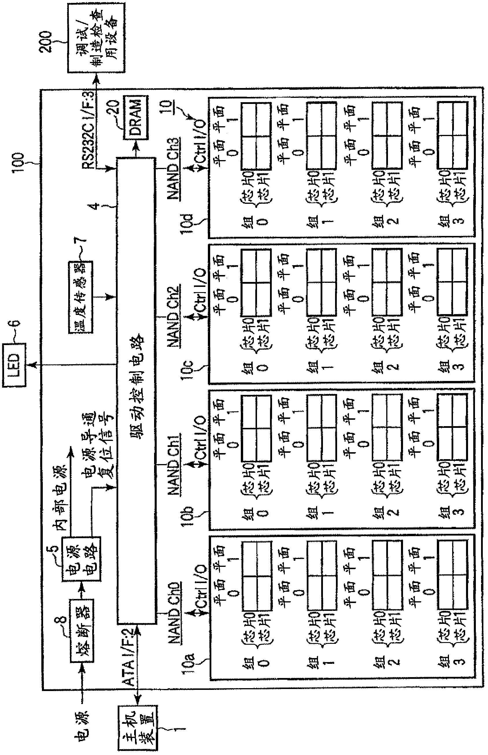
[0031] figure 1 It is a block diagram of a configuration example of SSD 100 as a storage system. The SSD 100 is connected to a host device (hereinafter referred to as host) 1 such as a personal computer or a CPU core through a memory connection interface such as an ATA interface (ATA I / F) 2 , and functions as an external memory of the host 1 . In addition, SSD 100 can transmit and receive data between debugging / manufacturing inspection devices 200 via communication interface 3 such as an RS232C interface (RS232C I / F).
[0032] SSD100 has: NAND type flash memory (hereinafter referred to as NAND memory) 10 as non-volatile semiconductor memory; drive control circuit 4 as controller; DRAM 20 as volatile semiconductor memory; power supply circuit 5; status display LED6 used; temperature sensor 7 to detect the temperature inside the driver; and fuse 8.
[0033] Power supply circuit 5 generates a plurality of different internal DC power supply voltages from an external DC power sup...
no. 2 Embodiment approach
[0126] Next, a second embodiment will be described. In the above-mentioned first embodiment, in order to reduce the influence of PD, RD, and DR, the management table MT is referred to, and the read levels VA, VB, VC and the read voltage Vread are changed in the + direction or the - direction to perform a read operation. After this read operation, ECC is judged, and when the number of error bits is large, the block is refreshed.
[0127] In contrast, the second embodiment performs offset reading (retry reading) when the number of error bits is too large to perform ECC error correction (ECC error) in ECC error correction at the time of initial reading. Moreover, by re-executing the ECC error correction, the defect rate of the system is improved.
[0128] Figure 13 , Figure 14 2nd Embodiment is shown. Such as Figure 13 As shown, first, data is read from a memory cell, for example, by a default read level (S31). Then, it is judged whether ECC error correction is possible ...
no. 3 Embodiment approach
[0145] Figure 15 3rd embodiment is shown. The third embodiment is a read operation in which the first and second embodiments are combined. That is, the monitoring reading described in the first embodiment is executed at power-on or at an arbitrary timing. In contrast, in the third embodiment, when an ECC error occurs during the read operation, the read level is shifted to both + / -, the read operation is performed, and the status data at that time is recorded in the management table. In the next read operation, the read operation is performed based on the state data recorded in the management table.
[0146] Such as Figure 15 As shown, for example, a read operation is performed with a default read level (S51). Then, it is judged whether ECC error correction is possible (S52). If the result of this determination is that an ECC error has occurred, first, for example, the read level is shifted slightly higher, and +offset read is performed (S53). After this reading, it is ...
PUM
 Abstract
Description
Claims
Application Information