Semiconductor light-emitting element manufacturing method, lamp, electronic device, and mechanical apparatus

A technology of light-emitting element and manufacturing method, which is applied in the direction of semiconductor devices, electrical components, lighting devices, etc., can solve the problems of p-type semiconductor layer obstacles and the lack of resistivity p-type semiconductor layers, etc.

Active Publication Date: 2012-05-30
TOYODA GOSEI CO LTD
View PDF5 Cites 0 Cited by
  • Summary
  • Abstract
  • Description
  • Claims
  • Application Information

AI Technical Summary

Problems solved by technology

[0004] However, in the case where an n-type semiconductor layer, an active layer, and a p-type semiconductor layer are sequentially laminated on a substrate, since these layers are formed in the same deposition chamber (growth chamber), the dopant used for forming the n-type semiconductor layer The dopant hinders the formation of the p-type semiconductor layer, and a p-type semiconductor layer with sufficiently low resistivity may not be obtained

Method used


Image

  • Semiconductor light-emitting element manufacturing method, lamp, electronic device, and mechanical apparatus
  • Semiconductor light-emitting element manufacturing method, lamp, electronic device, and mechanical apparatus
  • Semiconductor light-emitting element manufacturing method, lamp, electronic device, and mechanical apparatus

Examples


Embodiment 1

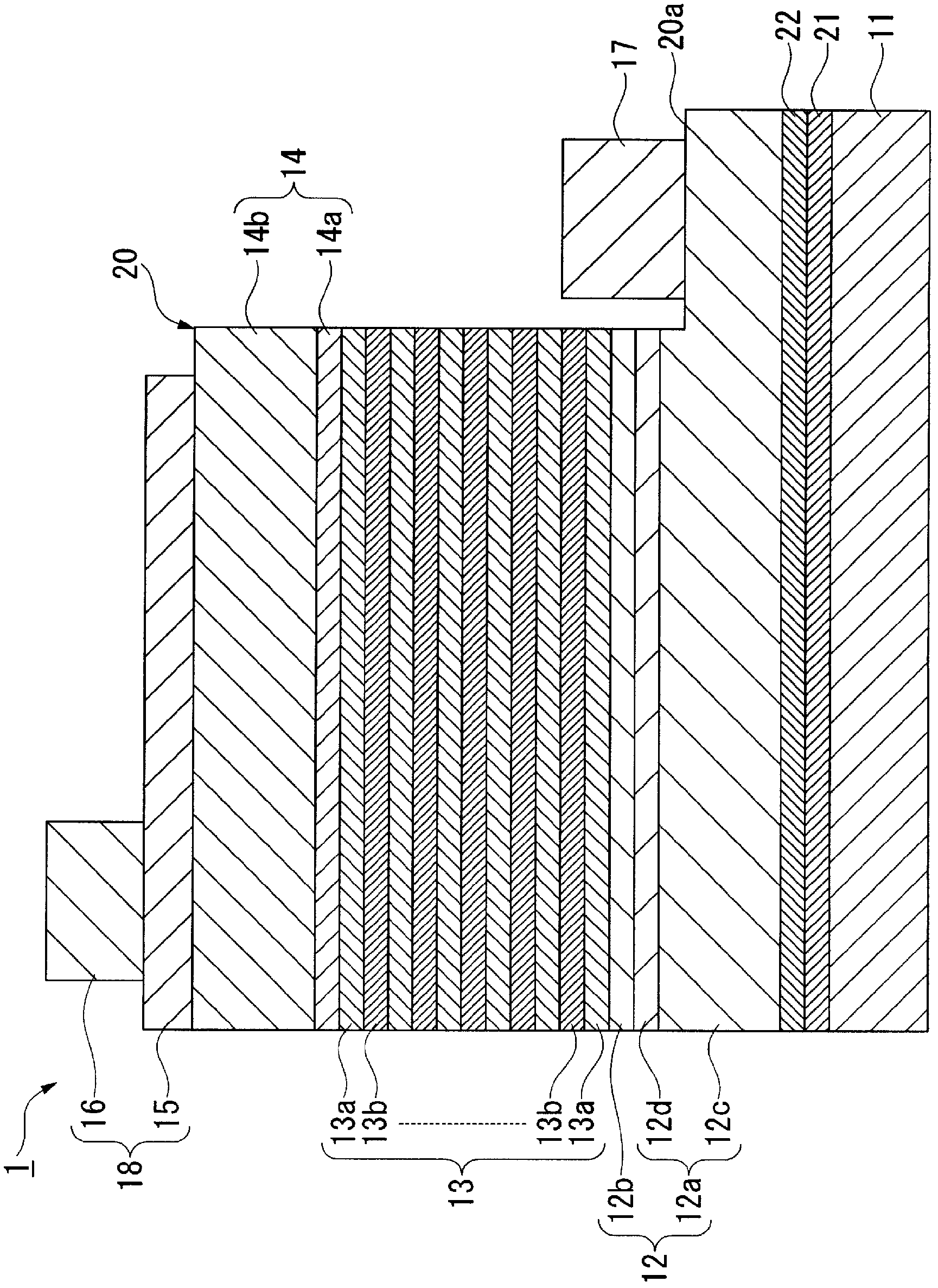
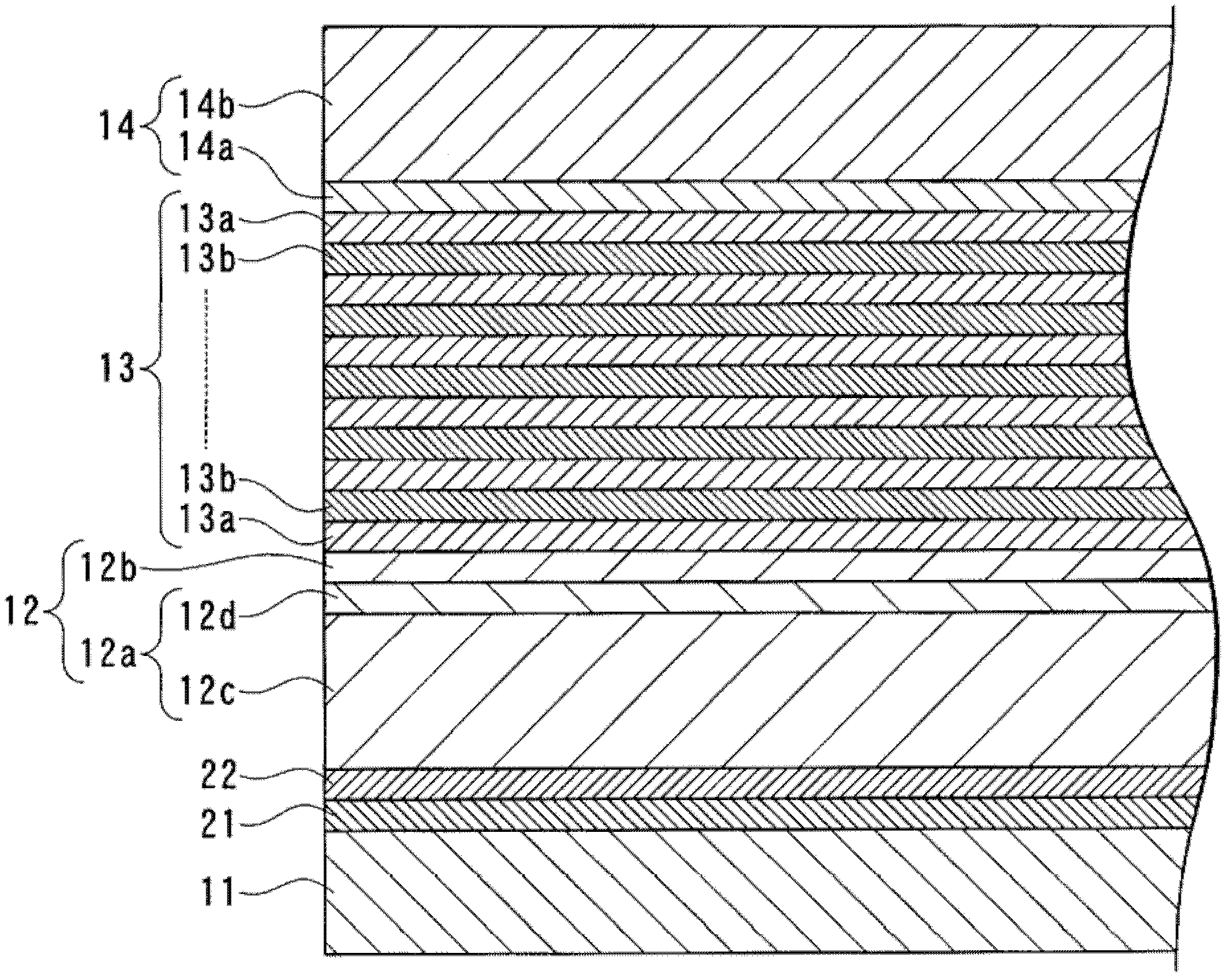
[0151] Using the method shown below, the figure 1 A semiconductor light emitting element 1 having the configuration shown.

[0152]In the manufacture of the semiconductor light-emitting element 1 of Example 1, first, on the top-view circular substrate 11 made of sapphire, the buffer layer 21 made of AlN; base layer 22; an n-contact layer with a thickness of 3.2 μm consisting of a first-step growth layer 12c made of Si-doped n-type GaN with a thickness of 3 μm and a re-growth layer 12d made of Si-doped n-type GaN with a thickness of 0.2 μm 12a; an n-cladding layer 12b of a superlattice structure with a thickness of 80 nm formed by repeatedly growing 20 layers (logarithmic) of the thin film layer composed of the n-side first layer and the n-side second layer, the n-side first layer It is composed of GaInN and has a thickness of 2nm, and the second n-side layer is composed of GaN and has a thickness of 2nm; the Si-doped GaN barrier layer with a thickness of 5nm and the In with a...

Embodiment 2

[0169] The n-cladding layer 12b is made of Ga 0.99 In 0.01 A semiconductor light-emitting element 1 was obtained in the same manner as in Example 1 except for the layer having a single-layer structure of N.

Embodiment 3

[0171] A semiconductor light-emitting element 1 was obtained in the same manner as in Example 1 except that the number of stacked thin film layers of the n-cladding layer 12b was 30 layers (30 pairs of layers (60 layers)).


PUM


Abstract

Disclosed is a semiconductor light-emitting element manufacturing method comprising a first step for stacking a first n-type semiconductor layer above a substrate in a first metalorganic chemical vapor deposition device, and a second step for sequentially stacking a regrowth layer, a second n-type semiconductor layer, an active layer, and a p-type semiconductor layer on the first n-type semiconductor layer in a second metalorganic chemical vapor deposition device.

Description

technical field [0001] The present invention relates to a manufacturing method of a semiconductor light emitting element, a lamp, an electronic device, and a mechanical device. [0002] This application claims priority based on Patent Application No. 2009-164004 filed in Japan on July 10, 2009 and Patent Application No. 2009-165993 filed in Japan on July 14, 2009, the contents of which are incorporated herein by reference middle. Background technique [0003] Conventionally, semiconductor light emitting elements used in light emitting diodes, semiconductor lasers, and the like include elements in which an n-type semiconductor layer, an active layer (light emitting layer) and a p-type semiconductor layer are sequentially stacked on a substrate. As a method of manufacturing such a semiconductor light-emitting element, there is a method of successively stacking n-type semiconductors sequentially and sequentially on a substrate made of sapphire single crystal or the like, using...

Claims


Application Information

Patent Timeline
Patent Type & Authority Applications(China)
IPC IPC(8): H01L33/12F21S2/00H01L33/32
CPCH01L33/02H01L33/007
Inventor 酒井浩光
Owner TOYODA GOSEI CO LTD
Why Eureka
Try Eureka