Nitride semiconductor device

A technology of nitride semiconductors and components, which is applied in the direction of semiconductor devices, semiconductor lasers, electrical components, etc., can solve problems such as crystallinity deviation, high output power, and difficulty in obtaining, and achieve the effect of improving luminous efficiency

Inactive Publication Date: 2007-04-04
NICHIA CORP
View PDF3 Cites 2 Cited by
  • Summary
  • Abstract
  • Description
  • Claims
  • Application Information

AI Technical Summary

Problems solved by technology

[0012] However, InGaN is difficult to grow into a film with few defects and good crystallinity, and it is difficult to obtain a desired ohmic contact with sufficiently low contact resistance.
In addition, there is also a problem that the contact resistance is unstable due to the crystallinity deviation of the formed InGaN layer.
Therefore, conventional nitride semiconductor devices having a p-type contact layer made of InGaN are difficult to obtain a sufficiently low and stable operating voltage and high output power at the same time
Therefore, for example, when constituting an LED element using a contact layer made of InGaN, there is a problem that the forward voltage (Vf) at 20mA cannot be as low as 3.4V to 3.8V, and the variation is large
[0013] In addition, elements made of nitride semiconductors may deteriorate even at a voltage of 100V, which is far lower than the static electricity generated by the human body, so care must be taken when handling them.

Method used


Image

  • Nitride semiconductor device
  • Nitride semiconductor device
  • Nitride semiconductor device

Examples


Embodiment approach 1

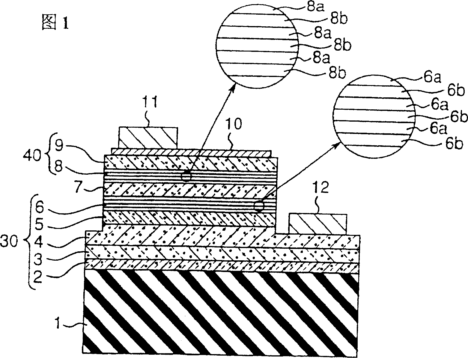
[0152] 1 is a schematic cross-sectional view showing the structure of a nitride semiconductor device (LED device) according to Embodiment 1 of the present invention. This LED element has a structure in which the following layers are sequentially stacked on a sapphire substrate 1: a first buffer layer 2 made of GaN; a second buffer layer 3 made of undoped GaN; The n-side contact layer 4 composed of; the third buffer layer 5 composed of non-doped GaN layer; the n-side multilayer film layer 6 composed of InGaN / GaN superlattice structure; the multiple quantum well composed of InGaN / GaN The active layer 7 of the structure; the p-side multilayer film layer 8 composed of AlGaN / GaN superlattice structure; the p-side contact layer 9 composed of Mg-doped GaN.

[0153] That is, the LED element of Embodiment 1 is formed on the sapphire substrate 1 by interposing the active layer 7 of the multi-quantum well structure between the n-side region 30 and the p-side region, the n-side region 30 ...

Embodiment approach 2

[0177] Next, referring to FIG. 4, a nitride semiconductor device according to Embodiment 2 of the present invention will be described.

[0178] The nitride semiconductor element of Embodiment 2 of the present invention is a light-emitting element having a double heterostructure on a substrate 1 having n-side regions 130 and The active layer 7 of the multi-quantum well structure sandwiched by the p-side region 140 .

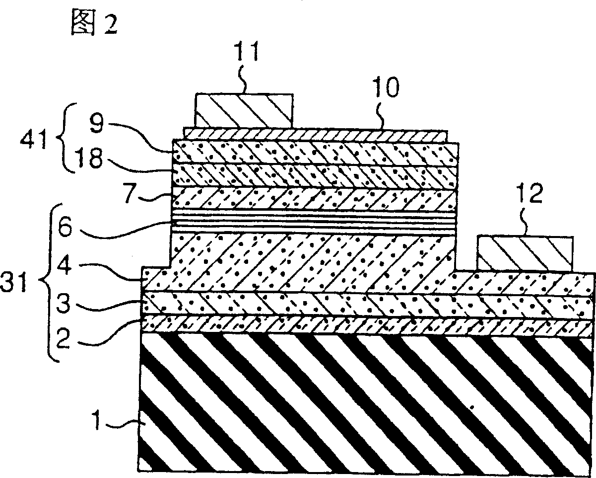
[0179] In detail, in the nitride semiconductor element of Embodiment 2, as shown in FIG. The contact layer 4, the n-side first multilayer film layer 105 containing n-type impurities, and the n-side second multilayer film layer 6 composed of the first nitride semiconductor film 106a and the second nitride semiconductor film 106b; the p-side The region 30 is composed of the p-side cladding layer 108 formed of a multi-layer film or a single-layer film and the p-side GaN contact layer 9 doped with Mg. In addition, in the nitride semiconductor device according to the...

Embodiment approach 3

[0241] Next, Embodiment 3 of the present invention will be described with reference to FIG. 5 .

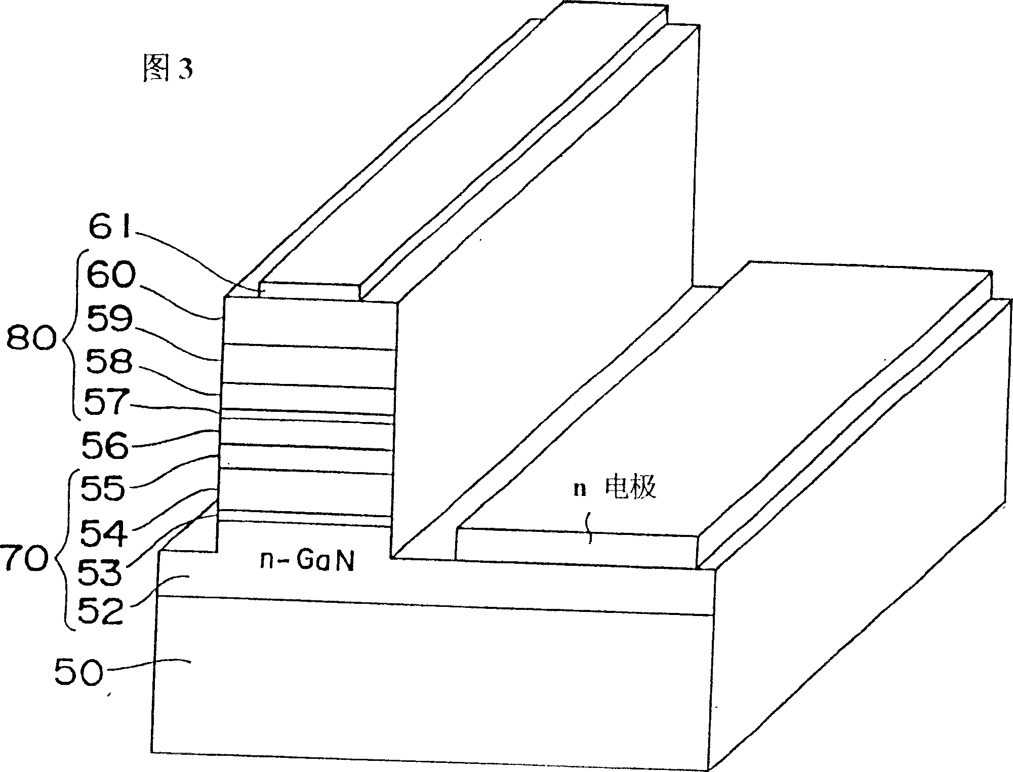
[0242] As shown in FIG. 5 , the nitride semiconductor light-emitting device according to Embodiment 3 of the present invention is structured as follows: On a substrate 1 made of, for example, sapphire, a first n-side nitride semiconductor layer 203 is sequentially formed via a buffer layer 202 , The second n-side nitride semiconductor layer 204 , the third n-side nitride semiconductor layer 205 , the active layer 7 , the p-side cladding layer 108 and the p-side contact layer 208 . Further, in the third embodiment, the light-transmitting p-electrode 10 is formed on substantially the entire upper surface of the p-side contact layer 208, and the p-pad electrode 11 for bonding is formed on a part of the p-electrode. In addition, the surface of the second n-side nitride semiconductor layer 204 is exposed on one side of the light-emitting element, and the n-electrode 12 is formed on the...


PUM


Abstract

According to the nitride semiconductor device with the active layer made of the multiple quantum well structure of the present invention, the performance of the multiple quantum well structure can be brought out to intensify the luminous output thereof thereby contributing an expanded application of the nitride semiconductor device. In the nitride semiconductor device comprises an n-region having a plurality of nitride semiconductor films, a p-region having a plurality of nitride semiconductor films, and an active layer interposed therebetween, a multi-film layer with two kinds of the nitride semiconductor films is formed in at least one of the n-region or the p-region.

Description

technical field [0001] The present invention relates to nitride semiconductors (for example, In x al y Ga 1-x-y N, 0≤x, 0≤y, x+y≤1) elements. Background technique [0002] Nitride semiconductors, as materials for high-brightness blue LEDs and pure green LEDs, have been practically used in various light sources such as full-color LED displays, traffic lights, and image scanner light sources. These LED elements basically have a structure in which the following layers are sequentially stacked on a sapphire substrate: a buffer layer made of GaN, an n-side contact layer made of GaN doped with Si, and a single quantum well structure (SQW: Single Quantum Well) with InGaN. -Quantum-Well) or an active layer with an InGaN multi-quantum well structure (MQW: Multi-Quantum-Well), a p-side cladding layer made of Mg-doped AlGaN, made of Mg-doped GaN The p-side contact layer; these components also show very excellent performance, that is, when the current is 20mA, the power is 5mW in th...

Claims


Application Information

Patent Timeline
Patent Type & Authority Applications(China)
IPC IPC(8): H01L33/00H01S5/343H01L33/32
Inventor 谷沢公二三谷友次中河義典高木宏典丸居宏充福田芳克池上武止
Owner NICHIA CORP
Why Eureka
Try Eureka