Luminous diode array

A technology of light-emitting diodes and arrays, applied in the field of light-emitting diode arrays, can solve problems such as low power consumption and achieve the effects of improving internal luminous efficiency, increasing luminous output power, and increasing luminous output power

Inactive Publication Date: 2004-09-08
HITACHI CABLE
View PDF2 Cites 0 Cited by
  • Summary
  • Abstract
  • Description
  • Claims
  • Application Information

AI Technical Summary

Problems solved by technology

[0009] However, in the above-mentioned light-emitting diode array, since the forward current I F It is limited to the current of the current path 19, so in order to obtain a certain luminous output power, a larger operating voltage is required, which cannot meet the requirements of low power consumption in recent years.

Method used


Image

  • Luminous diode array
  • Luminous diode array
  • Luminous diode array

Examples


Embodiment Construction

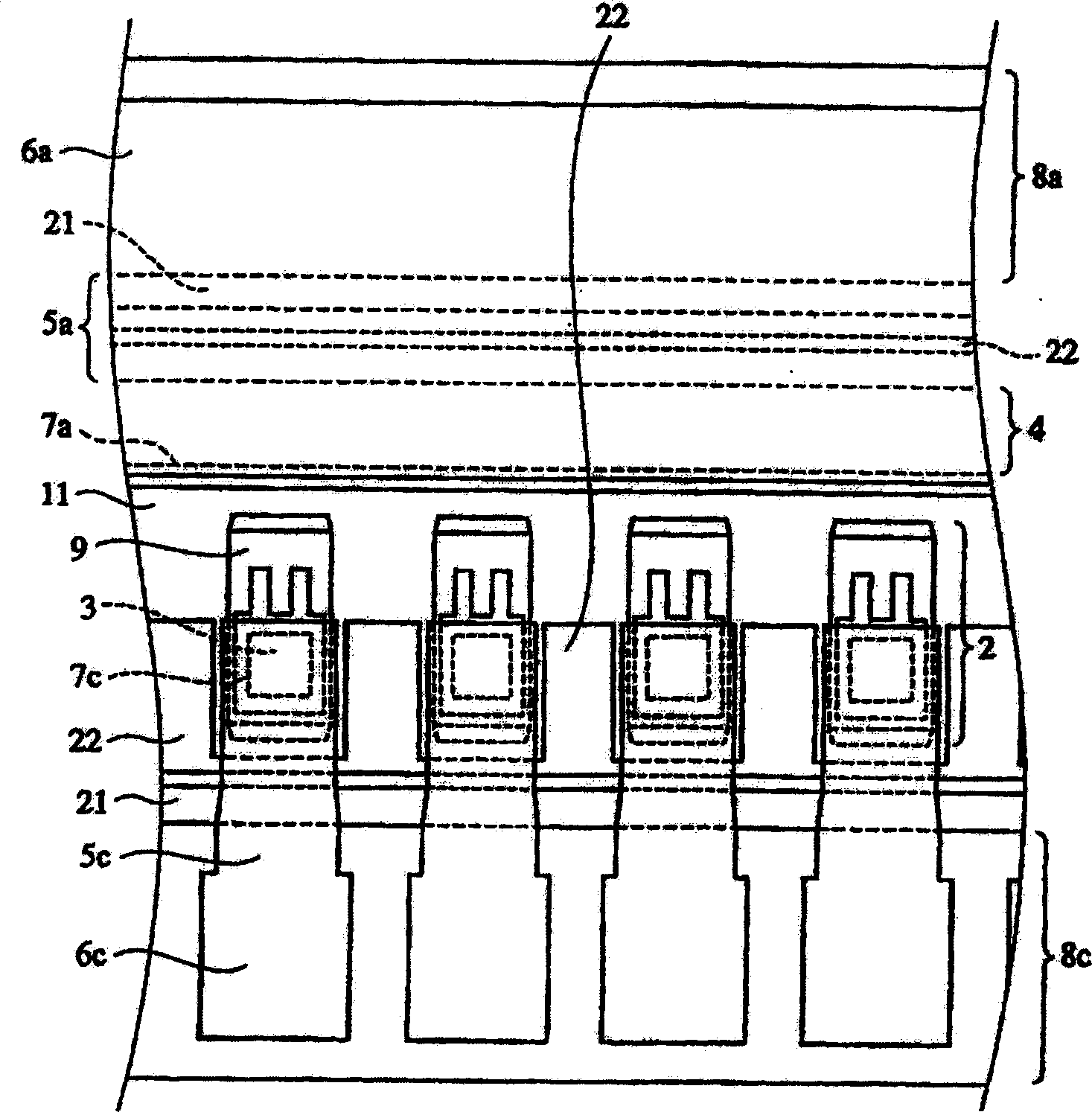
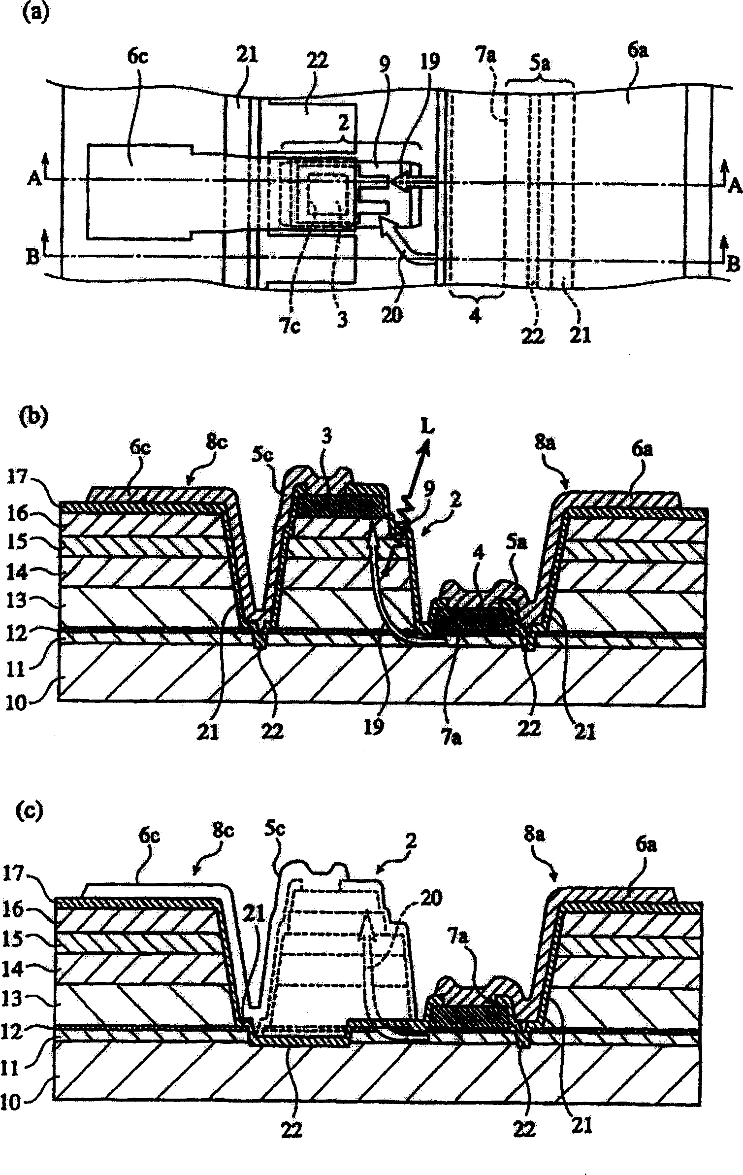
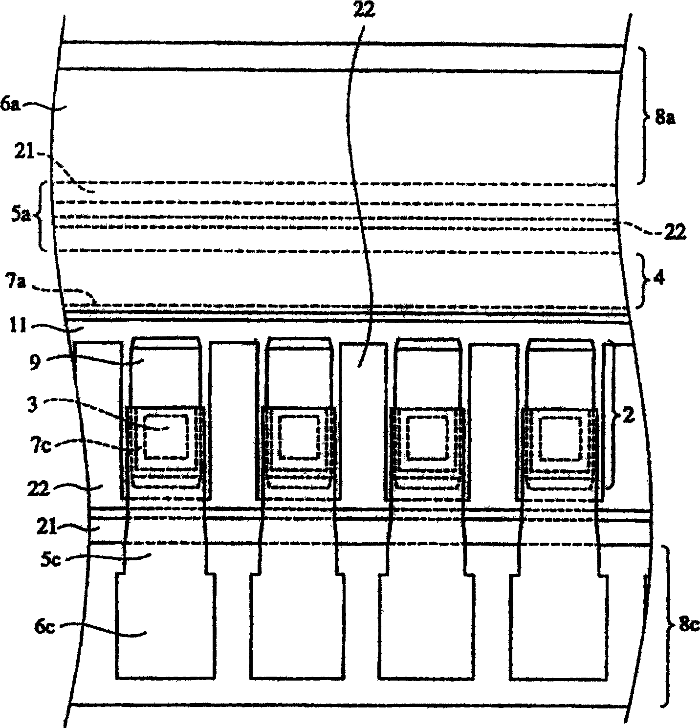
[0023] [1] Structure of LED array

[0024] Such as figure 1 as well as figure 2 As shown, the light-emitting diode array of the present invention has: a substrate 10, a plurality of light-emitting parts 2 formed on the substrate 10, a first electrode 3 formed on the upper surface of each light-emitting part 2, and a conductive layer 11. The second electrode 4 formed at a position close to the light emitting part 2 . In the illustrated embodiment, each light emitting part 2 is provided with a mesa etching groove on the epitaxial growth layer uniformly grown on the substrate 10, so that they become independent epitaxial growth layer parts.

[0025] (1) Substrate

[0026] The substrate 10 is not particularly limited as long as it is a material that can be used for a light-emitting diode, and any material can be electrically insulated from the light-emitting part. An n-type substrate or a p-type substrate can be used, and a semi-insulating substrate such as a semi-insulating...


PUM


Abstract

Provided is a diode array which reduces only the current in a sneak current path not contributing to light emission and allows increase in light emitting output and low-voltage operation. A light-emitting diode array comprising a conductive layer formed on a substrate; a plurality of separate light-emitting portions formed on the conductive layer; a first electrode formed on at least part of an upper surface of each of the light-emitting portions; and a second electrode formed on the conductive layer adjacent to the light-emitting portions, wherein the second electrode is a common electrode for operating the light-emitting portions, and wherein the conductive layer is removed in areas between adjacent light-emitting portions except for areas constituting current paths to the light-emitting portions.

Description

technical field [0001] The present invention relates to a light-emitting diode array with high light output power, especially a light-emitting diode array that can be suitably used as a light source for an electrophotographic printer. Background technique [0002] An electrophotographic printer forms an electrostatic latent image on a photosensitive drum with light corresponding to an image signal, selectively attaches toner to develop it, and transfers it to paper to obtain an image. As a light source for forming a latent image, a laser system and a light emitting diode array system are widely used. In particular, the light source of the light emitting diode array method is very suitable for small printers and large-scale printing because it does not require a long optical path like the laser method. In recent years, with the increase in printing speed and image quality and the miniaturization of printers, it is desired to obtain a higher-definition and high-power light-em...

Claims


Application Information

Patent Timeline
Patent Type & Authority Applications(China)
IPC IPC(8): H01L33/00H01L27/15
CPCH01L27/153
Inventor 行本富久
Owner HITACHI CABLE
Why Eureka
Try Eureka