Nitride semiconductor device
一种氮化物半导体、元件的技术,应用在半导体器件、半导体激光器、电气元件等方向,能够解决结晶性偏差、低工作电压、低接触电阻等问题,达到发光效率提高的效果
- Summary
- Abstract
- Description
- Claims
- Application Information
AI Technical Summary
Problems solved by technology
Method used
Image
Examples
Embodiment approach 1
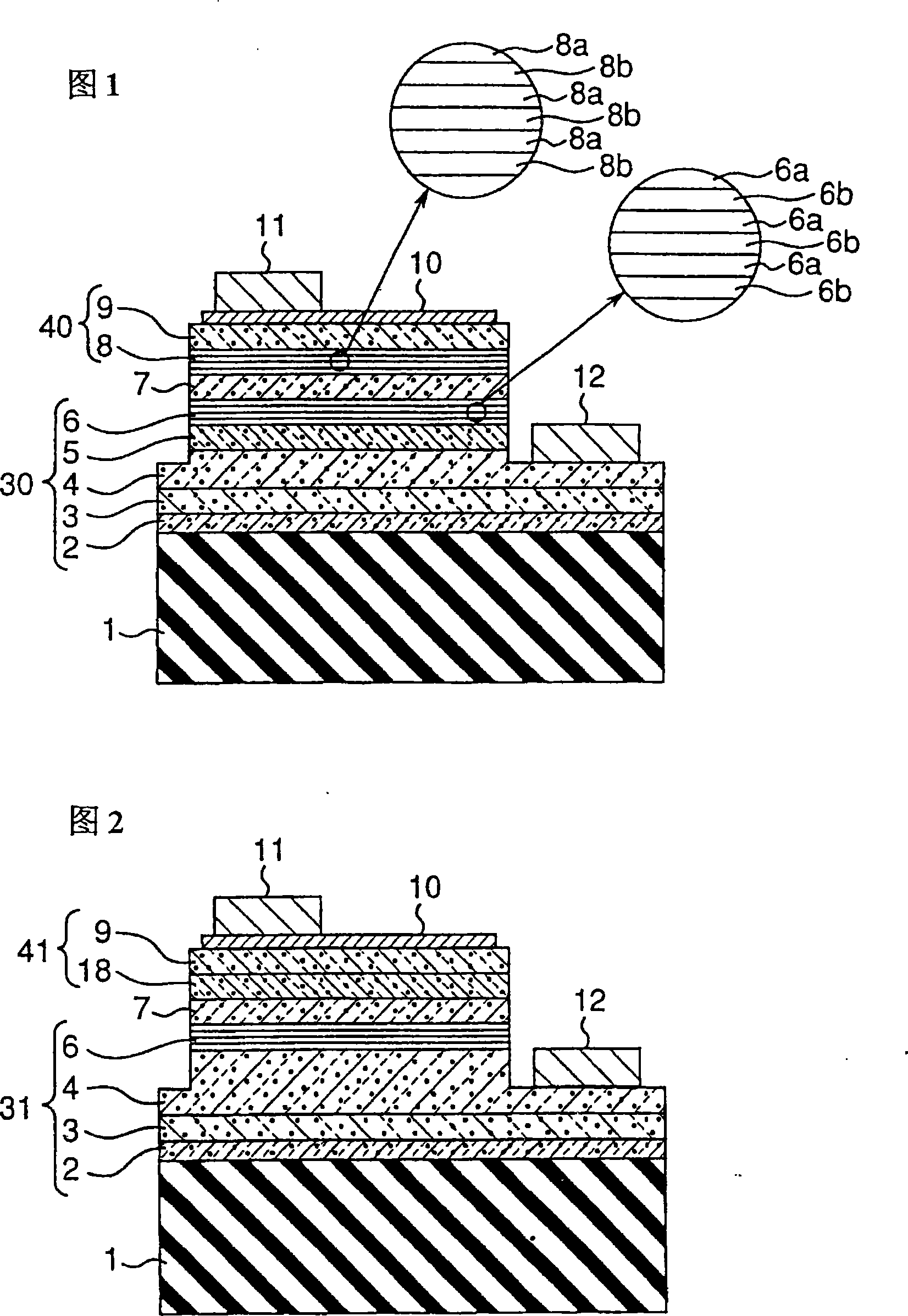
[0153] 1 is a schematic cross-sectional view showing the structure of a nitride semiconductor device (LED device) according to Embodiment 1 of the present invention. This LED element has a structure in which the following layers are sequentially stacked on a sapphire substrate 1: a first buffer layer 2 made of GaN; a second buffer layer 3 made of undoped GaN; The n-side contact layer 4 composed of; the third buffer layer 5 composed of non-doped GaN layer; the n-side multilayer film layer 6 composed of InGaN / GaN superlattice structure; the multiple quantum well composed of InGaN / GaN The active layer 7 of the structure; the p-side multilayer film layer 8 composed of AlGaN / GaN superlattice structure; the p-side contact layer 9 composed of Mg-doped GaN.
[0154] That is, the LED element of Embodiment 1 is formed on the sapphire substrate 1 by interposing the active layer 7 of the multi-quantum well structure between the n-side region 30 and the p-side region, the n-side region 30 ...
Embodiment approach 2
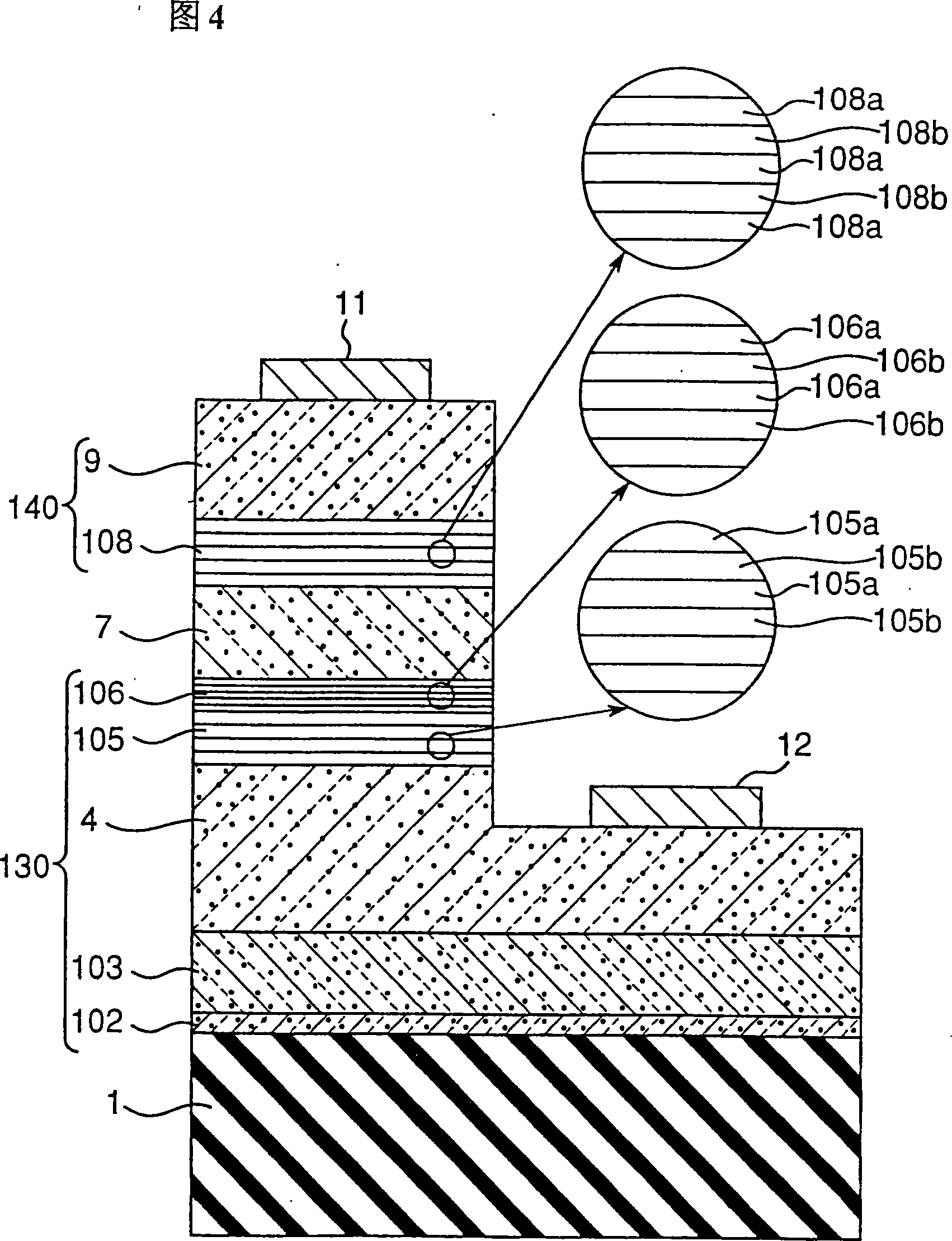
[0178] Next, referring to FIG. 4, a nitride semiconductor device according to Embodiment 2 of the present invention will be described.
[0179] The nitride semiconductor element of Embodiment 2 of the present invention is a light-emitting element having a double heterostructure on a substrate 1 having n-side regions 130 and The active layer 7 of the multi-quantum well structure sandwiched by the p-side region 140 .
[0180] In detail, in the nitride semiconductor device of Embodiment 2, as shown in FIG. 4, the n-side region 30 is composed of the following layers: a buffer layer 102, an undoped GaN layer 103, and an n-side region containing n-type impurities. The contact layer 4, the n-side first multilayer film layer 105 containing n-type impurities, and the n-side second multilayer film layer 6 composed of the first nitride semiconductor film 106a and the second nitride semiconductor film 106b; the p-side The region 30 is composed of the p-side cladding layer 108 formed of a...
Embodiment approach 3
[0242] Next, Embodiment 3 of the present invention will be described with reference to FIG. 5 .
[0243] As shown in FIG. 5 , the nitride semiconductor light-emitting device according to Embodiment 3 of the present invention is structured as follows: On a substrate 1 made of, for example, sapphire, a first n-side nitride semiconductor layer 203 is sequentially formed via a buffer layer 202 , The second n-side nitride semiconductor layer 204 , the third n-side nitride semiconductor layer 205 , the active layer 7 , the p-side cladding layer 108 and the p-side contact layer 208 . Further, in the third embodiment, the light-transmitting p-electrode 10 is formed on substantially the entire upper surface of the p-side contact layer 208, and the p-pad electrode 11 for bonding is formed on a part of the p-electrode. In addition, the surface of the second n-side nitride semiconductor layer 204 is exposed on one side of the light-emitting element, and the n-electrode 12 is formed on the...
PUM
| Property | Measurement | Unit |
|---|---|---|
| coating thickness | aaaaa | aaaaa |
| reflectivity | aaaaa | aaaaa |
| electrical resistivity | aaaaa | aaaaa |
Abstract
Description
Claims
Application Information


