Method for forming shallow-trench isolating structure

A technology of isolation structure and shallow trench, which is applied in the direction of electrical components, semiconductor/solid-state device manufacturing, circuits, etc., can solve the problem of poor step height consistency and achieve the effect of uniform density

Inactive Publication Date: 2012-06-06
SEMICONDUCTOR MANUFACTURING INTERNATIONAL (BEIJING) CORP
View PDF5 Cites 7 Cited by
  • Summary
  • Abstract
  • Description
  • Claims
  • Application Information

AI Technical Summary

Problems solved by technology

[0009] The problem solved by the invention is that the consistency of the step height is poor after forming the shallow trench isolation structure

Method used


Image

  • Method for forming shallow-trench isolating structure
  • Method for forming shallow-trench isolating structure
  • Method for forming shallow-trench isolating structure

Examples


Embodiment Construction

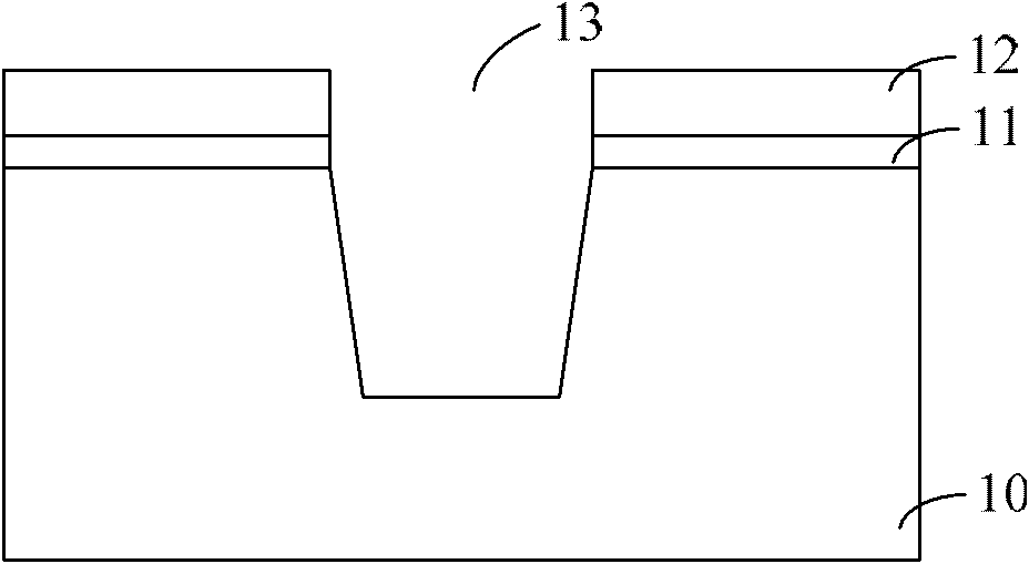
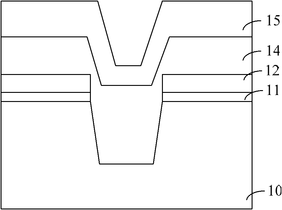
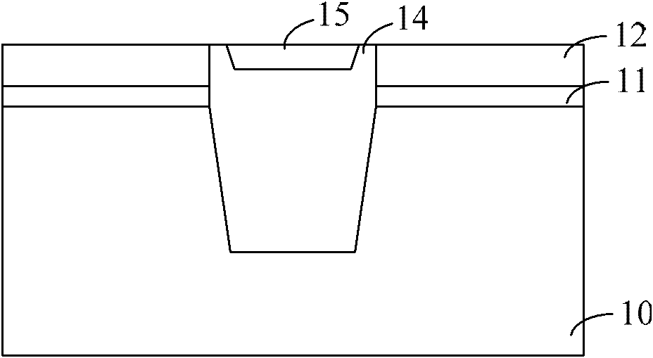
[0040] The formation process of the shallow trench isolation structure in the prior art is generally divided into two steps to fill the trench. First, a filling dielectric layer is formed to pre-fill the trench, and then a cap dielectric layer is formed on the filling dielectric layer to fill the trench. The trench is completely filled, but the formation process of the shallow trench isolation structure in the prior art will lead to the problem of poor step height uniformity.

[0041] After research, the inventor found that when forming the capping dielectric layer in the prior art, due to the high temperature of the high-density plasma chemical vapor deposition used, generally 700°C to 750°C, the previously formed filling dielectric layer The "parasitic" annealing effect increases the compactness of the filling dielectric layer after annealing, and due to the instability of the annealing effect, the filling dielectric layer between different shallow trench isolation structures...


PUM


Abstract

The invention relates to a method for forming a shallow-trench isolating structure. The method comprises the following steps of: providing a semiconductor substrate in which a trench is formed; forming a filling dielectric layer by using first high-density plasma chemical vapor deposition, carrying out prefilling on the trench and covering the surface of the semiconductor substrate; and forming a cap dielectric layer by using second high-density plasma chemical vapor deposition, carrying out complete filling on the trench and covering the filling dielectric layer, wherein the reaction temperature of the second high-density plasma chemical vapor deposition is 630-670 DEG C. The method contributes to improving the consistency of the step height and improving the performance of a device.

Description

technical field [0001] The invention relates to semiconductor manufacturing technology, in particular to a method for forming a shallow trench isolation structure. Background technique [0002] Active areas (active areas) of semiconductor devices such as MOS transistors are mostly isolated by a shallow trench isolation structure (STI, Shallow Trench Isolation). As the semiconductor technology enters the deep sub-micron era, the size of the shallow trench isolation structure is also reduced accordingly, and its aspect ratio is getting larger and larger. In the process of forming the shallow trench isolation structure, in order to improve the fillability, generally Dielectric filling is performed using High Density Plasma Chemical Vapor Deposition (HDPCVD). [0003] Figure 1 to Figure 4 A method for forming a shallow trench isolation structure in the prior art is shown. [0004] refer to figure 1 , providing a semiconductor substrate 10, on which a liner layer 11 and a ha...

Claims


Application Information

Patent Timeline
Patent Type & Authority Applications(China)
IPC IPC(8): H01L21/762H01L21/76
Inventor 平延磊
Owner SEMICONDUCTOR MANUFACTURING INTERNATIONAL (BEIJING) CORP
Why Eureka
Try Eureka