Regeneration process for dry etching lower electrode of LCD and AMOLED
An electrode and dry etching technology, which is applied in metal material coating technology, circuits, discharge tubes, etc., can solve the problems of high precision requirements and complex processing technology of the lower electrode, and achieve the effect of reducing costs and reducing the frequency of purchasing new electrodes
- Summary
- Abstract
- Description
- Claims
- Application Information
AI Technical Summary
Problems solved by technology
Method used
Image
Examples
Embodiment approach 1
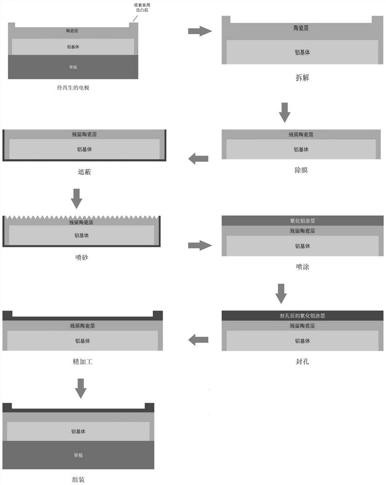
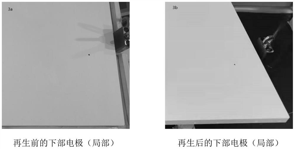
[0041] Such as figure 1 The bottom electrode of the dry-etched G6 AMOLED panel is shown. There are protrusions around the surface of this type of electrode, but there is no floating point. The real object before and after regeneration is as follows image 3 shown. The electrode regeneration process steps are as follows:
[0042] S1. Disassemble the electrode to be regenerated from the dry etching equipment, and remove the back plate and other components.
[0043] S2. Transfer and fix the electrode on the plane jig, and then transfer it to the gantry machining center together with the plane jig, adjust its flatness to within 50 microns, and then use a diamond tool to remove the surface part of the original ceramic coating on the electrode surface, The thickness removed was 600 microns.
[0044] S3. Transfer the electrode to the trolley, and cover the back and side of the electrode with heat-resistant glue to prevent it from being damaged or attached to the ceramic coating in...
Embodiment approach 2
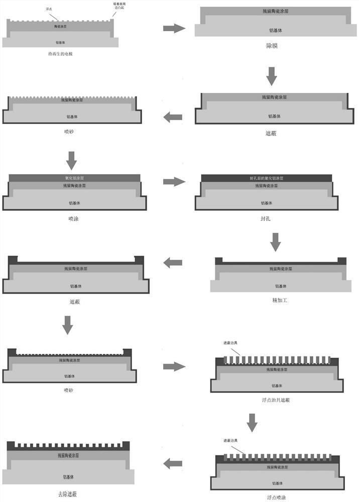
[0051] Process such as figure 2As shown, the lower electrode used for G5 LCD panel dry etching. There are protrusions around the surface of this type of electrode, and there are floating points in the middle. The diameter of the floating points is 2mm, and the spacing is 5mm. Figure 4 shown. The electrode regeneration process is as follows:
[0052] S1. Disassemble the electrode to be regenerated from the dry etching equipment, and remove other components.
[0053] S2. Transfer and fix the electrode on the plane jig, and then transfer it to the gantry machining center together with the plane jig, adjust its flatness to within 50 microns, and then use a diamond tool to remove the surface part of the original ceramic coating on the electrode surface, The thickness removed was 300 microns.
[0054] S3. Transfer the electrode to the trolley, and use a masking material to cover the back and side of the electrode to prevent it from being damaged or attached to the ceramic coat...
PUM
| Property | Measurement | Unit |
|---|---|---|
| thickness | aaaaa | aaaaa |
| height | aaaaa | aaaaa |
| width | aaaaa | aaaaa |
Abstract
Description
Claims
Application Information


