Method and device for accelerating emulation of CMP (Chemical Mechanical Polishing)

A technology of simulating data and grids, applied in the fields of instrumentation, calculation, electrical and digital data processing, etc., can solve the problems of restricting design efficiency, time-consuming, slow speed, etc.

Active Publication Date: 2012-06-20
INST OF MICROELECTRONICS CHINESE ACAD OF SCI
View PDF2 Cites 14 Cited by
  • Summary
  • Abstract
  • Description
  • Claims
  • Application Information

AI Technical Summary

Problems solved by technology

[0006] The scale of chip design shows the trend of system-on-chip (SOC) and network-level chip (NOC). times, and the corresponding physical layout data reaches dozens of Gb (10 9 Bits), or even hundreds of Gb, it is a very time-consuming task to perform CMP simulation on such a large-scale physical layout. In the iterative process of physical design-CMP simulation-correction-re-simulation-re-correction, the speed of CMP simulation It is one of the important factors affecting the design cycle of integrated circuits. Traditional serial and parallel CMP simulations need to make detailed and complex simulation calculations for each tiny area of ​​the integrated circuit layout, so the speed is relatively slow, which restricts the improvement of design efficiency.

Method used


Image

  • Method and device for accelerating emulation of CMP (Chemical Mechanical Polishing)
  • Method and device for accelerating emulation of CMP (Chemical Mechanical Polishing)
  • Method and device for accelerating emulation of CMP (Chemical Mechanical Polishing)

Examples


Embodiment Construction

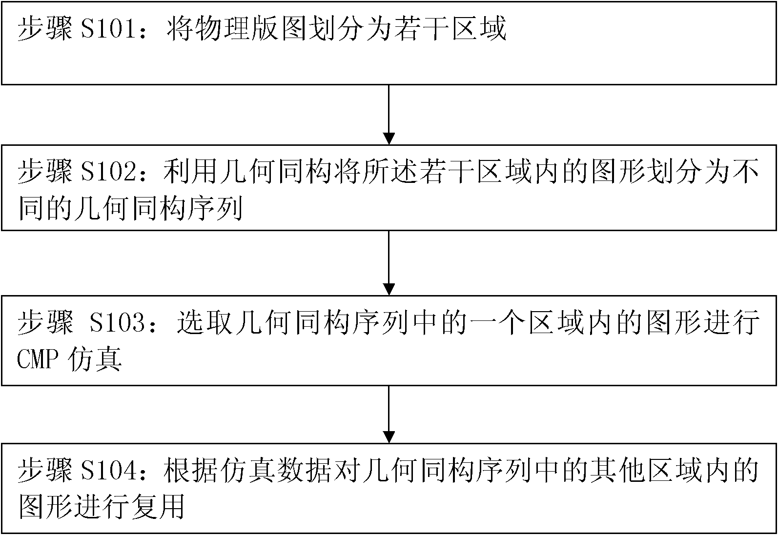
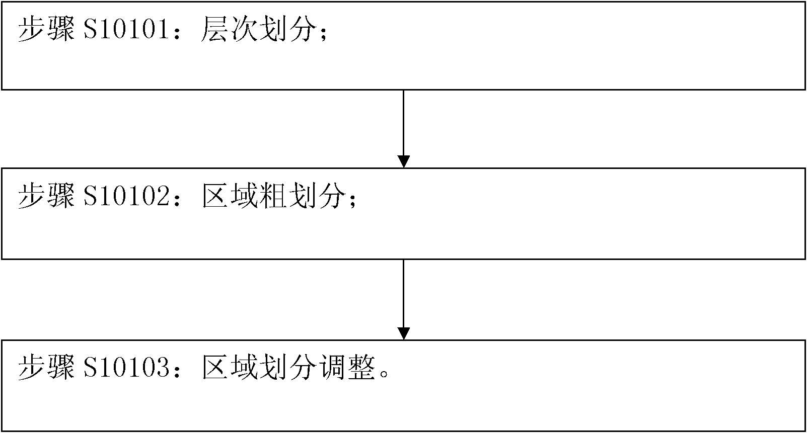
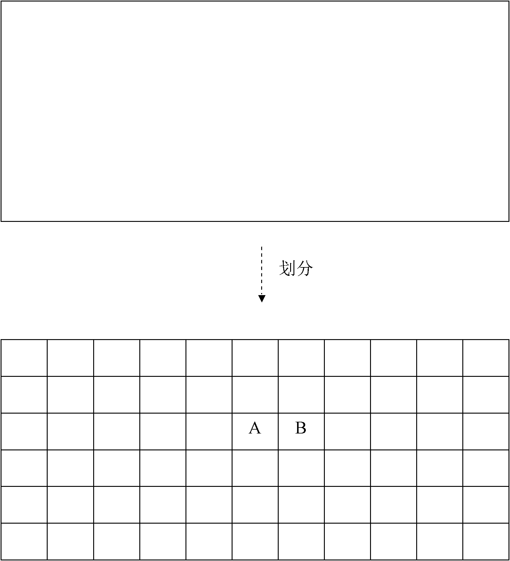
[0041] In the physical design of integrated circuits, there is a great similarity in the design graphics between local areas, which determines the sameness of the CMP calculation process and calculation results between local areas, and the multiplexing of calculation results can effectively reduce the Complicated simulation calculation tasks can improve the overall CMP simulation speed of the chip without sacrificing simulation accuracy. The present invention performs CMP simulation on different regions in a parallel manner to improve the CMP simulation speed of the whole chip and shorten the time required for the whole chip by dividing the physical layout area, the geometric isomorphism of the graphics in the area, the CMP simulation in the area, and the multiplexing of the area CMP simulation data. The CMP simulation time of the whole chip; the CMP simulation tasks are merged in the way of graph isomorphism, and the CMP simulation tasks of the same physical layout are calcula...


PUM


Abstract

The invention discloses a method and a device for accelerating the emulation of a CMP (Chemical Mechanical Polishing). The method for accelerating the emulation of the CMP comprises the following steps of: firstly, dividing a physical layout into a plurality of areas; secondly, dividing graphs in the areas into different geometry isomorphic sequences by using a geometry isomorphism; thirdly, selecting the graph in one area of the geometry isomorphic sequence for carrying out CMP emulation; fourthly, multiplexing the graphs in other areas in the geometry isomorphic sequences according to emulation data. According to the method and the device disclosed by the invention, through the division of the physical layout, the geometry isomorphism of the graphs in the areas, the CMP emulation in the areas and the multiplexing of CMP emulation data in the areas, the emulation speed of the CMP of a whole chip is increased and the emulation time of the CMP of the whole chip is shortened; and a CMP emulation task is merged in a graph isomorphic way; and on the basis of the graph isomorphism, primary calculation for the same CMP emulation task of the physical layout is carried out and the emulation result of the CMP is multiplexed, and thereby the emulation speed of the CMP of the whole chip is increased by reducing the quantity of the CMP emulation tasks.

Description

technical field [0001] The invention relates to the field of integrated circuit design automation, in particular to a method and device for accelerating CMP simulation. Background technique [0002] The manufacturing process of copper as an interconnection needs to etch the interconnection trenches and vias after the deposition of oxide materials; then deposit a thin barrier metal layer that is conducive to the growth of copper films as a seed layer; The electroless plating (ECP) method deposits copper into the interconnection trenches and vias; finally, removes excess copper outside the trenches and vias to produce an interconnection pattern. [0003] Chemical Mechanical Polishing (CMP) is a technique that removes excess copper and flattens the surface of silicon wafers. Therefore, in the integrated circuit manufacturing process in which metal copper is used as interconnection lines, CMP for planarizing the surface of silicon wafers is one of the important steps in the pr...

Claims


Application Information

Patent Timeline
Patent Type & Authority Applications(China)
IPC IPC(8): G06F17/50
Inventor 陈岚阮文彪吴玉平
Owner INST OF MICROELECTRONICS CHINESE ACAD OF SCI
Why Eureka
Try Eureka