Method for eliminating internal nodes of metal-oxide-semiconductor field effect transistor (MOSFET) used in rapid circuit simulation

A technology of internal nodes and nodes, applied in the direction of electrical digital data processing, special data processing applications, instruments, etc., can solve the problem of losing necessity

Inactive Publication Date: 2010-12-01
北京华大九天科技股份有限公司
View PDF3 Cites 12 Cited by
  • Summary
  • Abstract
  • Description
  • Claims
  • Application Information

AI Technical Summary

Problems solved by technology

Then, this method also loses the necessity

Method used


Image

  • Method for eliminating internal nodes of metal-oxide-semiconductor field effect transistor (MOSFET) used in rapid circuit simulation
  • Method for eliminating internal nodes of metal-oxide-semiconductor field effect transistor (MOSFET) used in rapid circuit simulation
  • Method for eliminating internal nodes of metal-oxide-semiconductor field effect transistor (MOSFET) used in rapid circuit simulation

Examples


Embodiment Construction

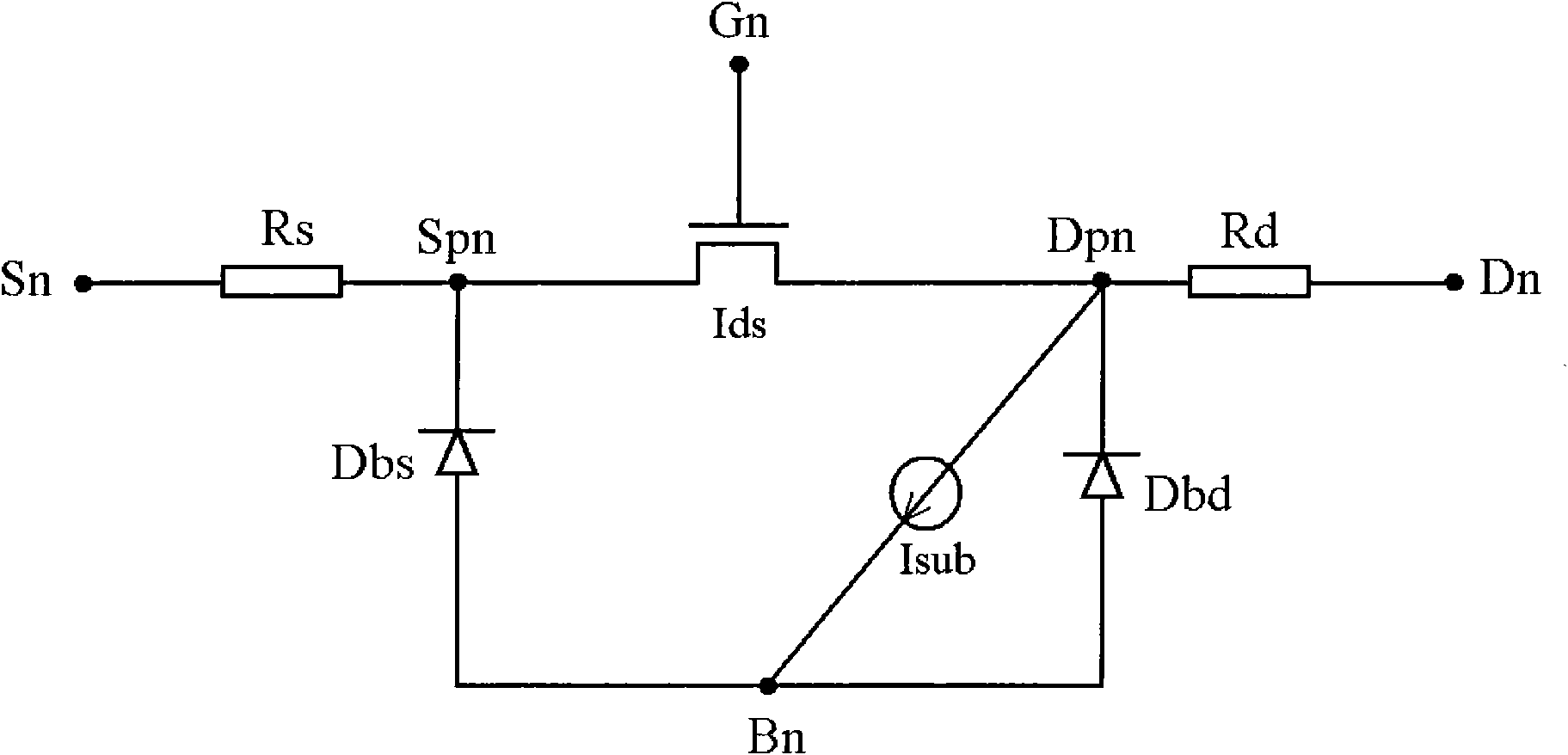
[0056] MOSFET is a 4-terminal device such as figure 1 As shown, its external nodes are Dn, Gn, Sn and Bn respectively. When the parasitic resistance R of the Dn terminal and the Sn terminal d and R s When it cannot be ignored, we will use a 6-node circuit network to equivalent MOSFET, and these 6 nodes are Dn, Dpn, Sn, Spn, Gn and Bn respectively. Also included in this circuit network are Ids (the intrinsic part of MOSFET), two current sources of Isub and two diodes of Dbs and Dbd.

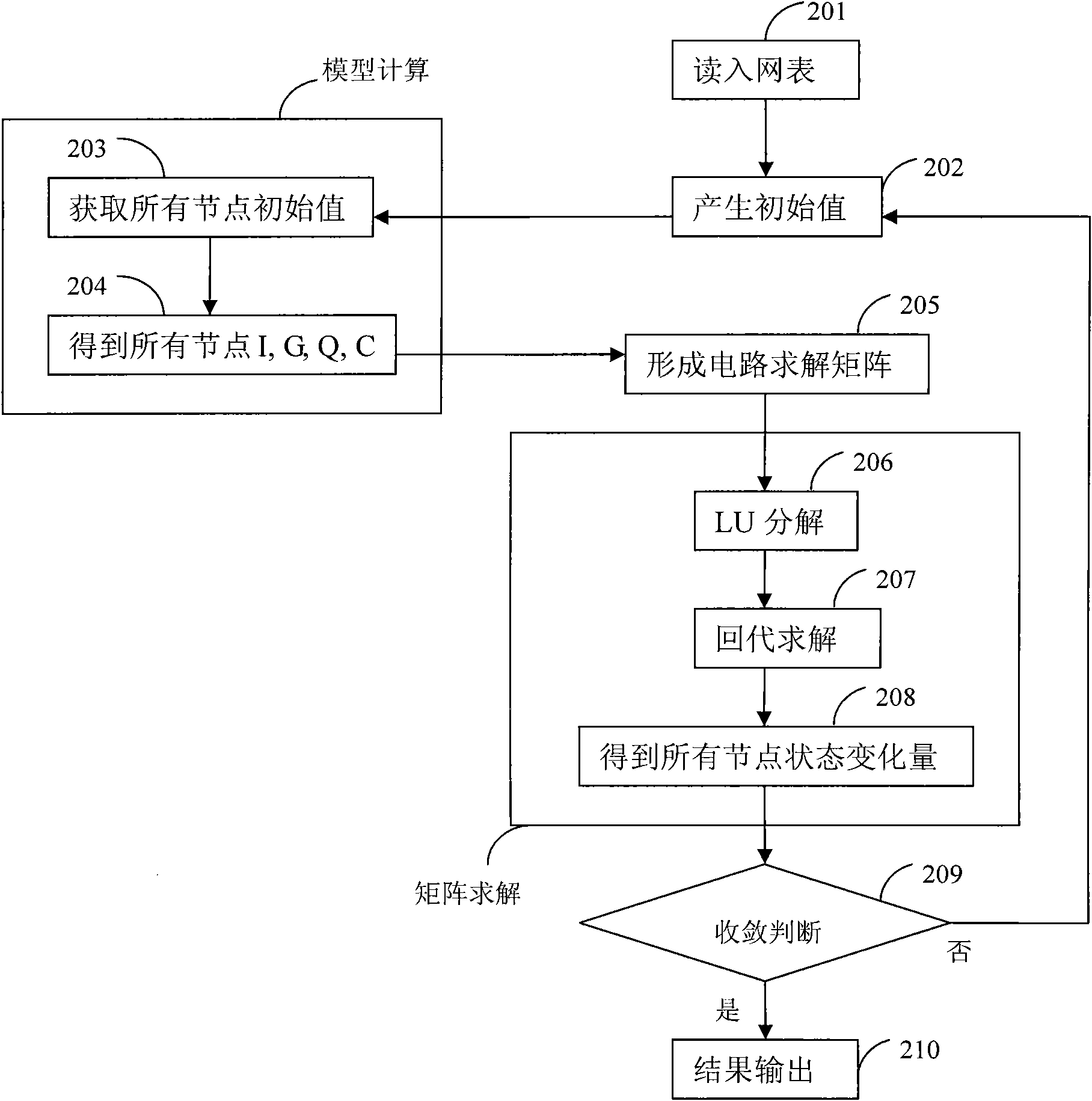
[0057] If a circuit contains such figure 1 6-node MOSFET shown, then the conventional circuit simulation flow is as follows figure 2 shown. The circuit simulator first reads in the netlist (201), and then generates a set of voltages and branch currents of all nodes (including internal nodes of MOSFETs) of each device for model calculation, which is the initial value of the circuit (202). Give this group of circuit state initial values ​​to the model Engine (203), enter the model calculation...


PUM


Abstract

The invention provides a method for eliminating internal nodes of a metal-oxide-semiconductor field effect transistor (MOSFET) used in rapid circuit simulation. The method comprises the following steps of: making a 4-node MOSFET model which does not comprise any internal node equivalent to a 6-node MOSFET model which comprises internal nodes in a circuit simulation process; solving the voltages of two internal nodes of the MOSFET by an analytic method; calculating the change of an internal node voltage along with an external node voltage; and finally obtaining a transient conductance relation among external nodes of all apparatuses used in matrix calculation. The method has the advantages of ensuring circuit simulation accuracy by considering the effect of MOSFET parasitic resistance on an electrical property, eliminating the internal nodes of the MOSFET, reducing a circuit solving matrix, reducing matrix solving time and increasing circuit simulation speed.

Description

1. Technical field [0001] The present invention belongs to the field of EDA (Electronic Design Automation). In particular, it relates to a method for establishing and simulating a MOSFET model considering eliminating internal nodes in fast circuit simulation. 2. Technical background [0002] The design of integrated circuits is inseparable from the simulation and verification of the designed circuits with a simulator. The process of circuit simulation is to first establish electrical equations on each node of the entire circuit network according to the device model and Kirchhoff's law. Generally speaking, this is a set of nonlinear equations, and then through Newton- Raphson (Newton-Ralphson) iteratively solves this group of equations to obtain simulation results. This process can be expressed as: [0003] G·ΔV=I [0004] Among them, the vector I is the current of each node, the matrix G is the transient derivative of the node current to the node voltage, and the vector ...

Claims


Application Information

Patent Timeline
Patent Type & Authority Applications(China)
IPC IPC(8): G06F17/50
Inventor 尚也淳侯文婷吴大可
Owner 北京华大九天科技股份有限公司
Why Eureka
Try Eureka