

Manufacturing method of electroluminescence test electrode
A technology for testing electrodes and manufacturing methods, which is applied to measuring devices, measuring electrical variables, and manufacturing measuring instruments, etc., can solve the problems of poor test repeatability, difference, and poor optical power test repeatability, and achieve improved repeatability, convenient use and reliability. The effect of stabilizing photoelectric test results
- Summary
- Abstract
- Description
- Claims
- Application Information
AI Technical Summary
Problems solved by technology
Method used
Image

Examples
Embodiment 1
[0021] A method for manufacturing an electroluminescence test electrode, comprising the following steps:
[0022] (1) Select a batch of indium particles with a diameter of 0.65mm, and the diameter tolerance is within 5%;
[0023] (2) Use a fixed pressure on the epitaxial wafer to press the above-mentioned indium particles with a constant force, and the tolerance of the pressure is less than 1%; the material for pressing the indium particles is the polished surface of the aluminum oxide substrate, and the roughness is Ra≥5um;
[0024] (3) Then heat the indium particles at 380°C for 2 minutes, cool for 1 minute, press for 5 seconds, and cycle 3 times to stabilize the resistance between the indium particles and the epitaxial wafer, and the tolerance of voltage and resistance is less than 5%. ;
[0025] (4) Finally, test on the electroluminescence tester.
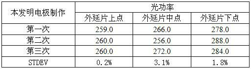
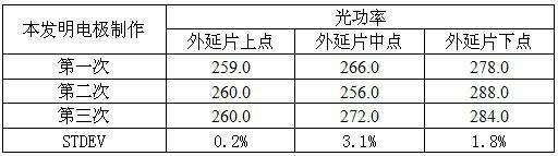
[0026] The optical power results of the test are shown in the table below.
[0027] Table 1 adopts the electrode manufactu...
Embodiment 2
[0034] A method for manufacturing an electroluminescence test electrode, comprising the following steps:
[0035] (1) Select a batch of indium particles with a diameter of 0.30mm, and the diameter tolerance is within 5%;
[0036] (2) Use a fixed pressure on the epitaxial wafer to press the above-mentioned indium particles with a constant force, and the tolerance of the pressure is less than 1%; the material for pressing the indium particles is the polished surface of the aluminum oxide substrate, and the roughness is Ra≥5um;
[0037] (3) Heat the indium pellets at 400°C for 1 minute, cool for 0.5 minutes, press for 2 seconds, and cycle twice to stabilize the resistance between the indium pellets and the epitaxial wafer, and the tolerance of voltage and resistance is less than 5%;
[0038] (4) Finally, test on the electroluminescence tester.
[0039] The measured optical power results are shown in Table 3.
[0040] Table 3 adopts the electrode manufacturing method of the pres...
Embodiment 3
[0044] A method for manufacturing an electroluminescence test electrode, comprising the following steps:
[0045] (1) Select a batch of indium particles with a diameter of 0.65mm, and the diameter tolerance is within 5%;
[0046] (2) Use a fixed pressure on the epitaxial wafer to press the indium pellets with a constant force, and the tolerance of the pressure is less than 1%; the material for pressing the indium pellets is the polished surface of the aluminum oxide substrate, and the roughness is Ra≥5um;
[0047] (3) Heat the indium particles at 350°C for 3 minutes, cool for 2 minutes, press each electrode for 8 seconds, and cycle twice to stabilize the resistance between the indium particles and the epitaxial wafer, and the tolerance of voltage and resistance is less than 5 %;
[0048] (4) Finally, test on the electroluminescence tester.
[0049] The measured optical power results are shown in Table 4.
[0050] Table 4 adopts the electrode manufacturing method of the pres...
PUM
 Abstract
Description
Claims
Application Information