Input output (IO) interface output circuit in microprocessor

An output circuit and microprocessor technology, applied in the direction of electrical digital data processing, instruments, etc., can solve the problems of increasing circuit hardware overhead, increasing circuit area, increasing the number of electronic components, etc., to achieve the effect of saving hardware overhead

Inactive Publication Date: 2012-06-27
SHENZHEN STATE MICROELECTRONICS CO LTD
View PDF3 Cites 13 Cited by
  • Summary
  • Abstract
  • Description
  • Claims
  • Application Information

AI Technical Summary

Problems solved by technology

However, the direct defect of this solution is that the circuit area increases and the num

Method used


Image

  • Input output (IO) interface output circuit in microprocessor
  • Input output (IO) interface output circuit in microprocessor
  • Input output (IO) interface output circuit in microprocessor

Examples


Example Embodiment

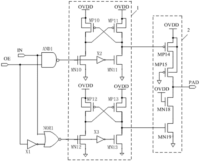
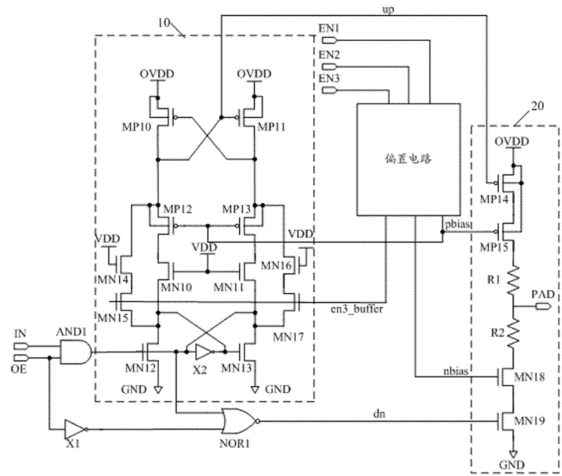
[0023] like figure 2 As shown, the present invention proposes an IO interface output circuit that can adapt to multiple IO power supplies and have multiple drive capabilities in a microprocessor under a deep submicron process, which includes: a level conversion circuit 10, a drive circuit 20, a bias Setting circuit, a 2-input AND gate AND1, a 2-input NOR gate NOR1 and an inverter X1. The connection relationship is as follows: the two input terminals of the AND gate AND1 are respectively connected to the data output signal IN and the enable output signal OE, and the output terminal of the AND gate AND1 is connected to the input terminal of the level conversion circuit 10 (ie, the gate of the transistor MN12); The output of the AND gate AND1 is also connected to one of the input terminals of the NOR gate NOR1; the input terminal of the inverter X1 is connected to the enable output signal OE, and the output terminal is connected to the other input terminal of the NOR gate NOR1; ...


PUM


Abstract

The invention discloses an input output (IO) interface output circuit in a microprocessor, which comprises a level switch circuit used for converting a core power supply VDD in the microprocessor into an IO power supply OVDD with different voltage, a biasing circuit used for generating and outputing biasing signals pbias and nbias and a bypass enable signal and a driving circuit used connecting the biasing signal pbias and the biasing signal nbias. The level switch circuit comprises a switch network and a bypass circuit both connected with the core power supply VDD. The biasing signal pbias and the bypass enable signal are respectively output to the switch network and the bypass circuit, the switch network adapts to the IO power supply OVDD with different voltage by changing voltage of the biasing signal pbias, and the bypass enable signal controls connection of the bypass circuit when the IO power supply OVDD is equal to the core power supply VDD. The IO interface output circuit outputs the biasing signal pbias and nbias with different voltage through the biasing circuit, enables an IO circuit to have different driving capability and greatly saves hardware expense in design of the circuit.

Description

technical field [0001] The invention relates to an IO (Input and Output) interface output circuit, in particular to an IO interface output circuit capable of adapting to multiple IO power sources and having multiple driving capabilities in a microprocessor under a deep submicron process. Background technique [0002] like figure 1 As shown, in the current microprocessor IO interface output circuit, the data output signal IN and the enable output signal OE pass through a NAND gate AND1 and NOR gate NOR1 (the output enable signal OE enters the OR through an inverter X1 The control of one of the input terminals of the NOT gate NOR1) is transmitted to the level conversion circuit 1 to convert it into an IO high-voltage signal, and then output to the PAD through the driving circuit 2. [0003] Wherein, the flat switching circuit 1 includes 2 switching networks: the first switching network consisting of 2 N-type transistors MP10 and MP11, 2 N-type transistors MN10 and MN11, and a...

Claims


Application Information

Patent Timeline
IPC IPC(8): G06F13/20
Inventor 胡伟平康海容
Owner SHENZHEN STATE MICROELECTRONICS CO LTD
Why Eureka
Try Eureka