Systems and methods for locating defective components of a circuit

a technology of defective components and circuits, applied in the field of diagnostics, can solve the problems of reducing the reliability of traditional reliability circuit screening methods, affecting the reliability of chips, and increasing scaling, so as to reduce the time for diagnosis, improve efficiency, and reduce hardware overhead

Active Publication Date: 2012-07-03
NEC CORP
View PDF4 Cites 5 Cited by
  • Summary
  • Abstract
  • Description
  • Claims
  • Application Information

AI Technical Summary

Benefits of technology

[0011]One advantage of applying exemplary features of the present principles is that they permit the application of a scan chain across different field repairable units. Moreover, responses of all FRUs may be observed simultaneously, thereby reducing diagnosis time. For example, defective tiles are discoverable at any tile location and in any quantity within a maximal capacity in one pass of a set of test patterns. In addition, efficiency may be further improved by exploiting the fact that registers process data at a rate that is faster than a scan shift rate of a circuit under diagnosis. Thus, certain exemplary space-compression circuit systems with reduced hardware overhead may be implemented by exploiting a frequency difference between a scan shift clock and a system clock.

Problems solved by technology

However, despite these improvements, increased scaling may detrimentally affect chip reliability due to elevated chip temperature resulting from increased power density and leakage current.
In addition, scaling has a significant impact on hard fault rates.
Leakage current stemming from scaling reduces the reliability of traditional reliability circuit screening methods such as burn-in and IDD, testing.
As such, screening all defective chips is extremely difficult and expensive for large chips.
With regard to deep submicron technology, there are many defects that cannot be detected with existing fault models.
Furthermore, even if a test technique is able to screen and detect 100% of defective chips, working chips may become defective before their expected life spans as a result of power surge, human mistakes, and other factors.
Although redundancy-based fault tolerance techniques have been used in systems that require high reliability, these techniques are less attractive solutions mainly due to the increase in power consumption resulting from their use.
Thus, if the board includes many chips, a long diagnosis time is required.
However, existing techniques fail to identify defective blocks that have varying sizes within a chip.
Furthermore, existing techniques fail to provide a means for processing a large number of responses in parallel with low hardware complexity.

Method used


Image

  • Systems and methods for locating defective components of a circuit
  • Systems and methods for locating defective components of a circuit
  • Systems and methods for locating defective components of a circuit

Examples


Embodiment Construction

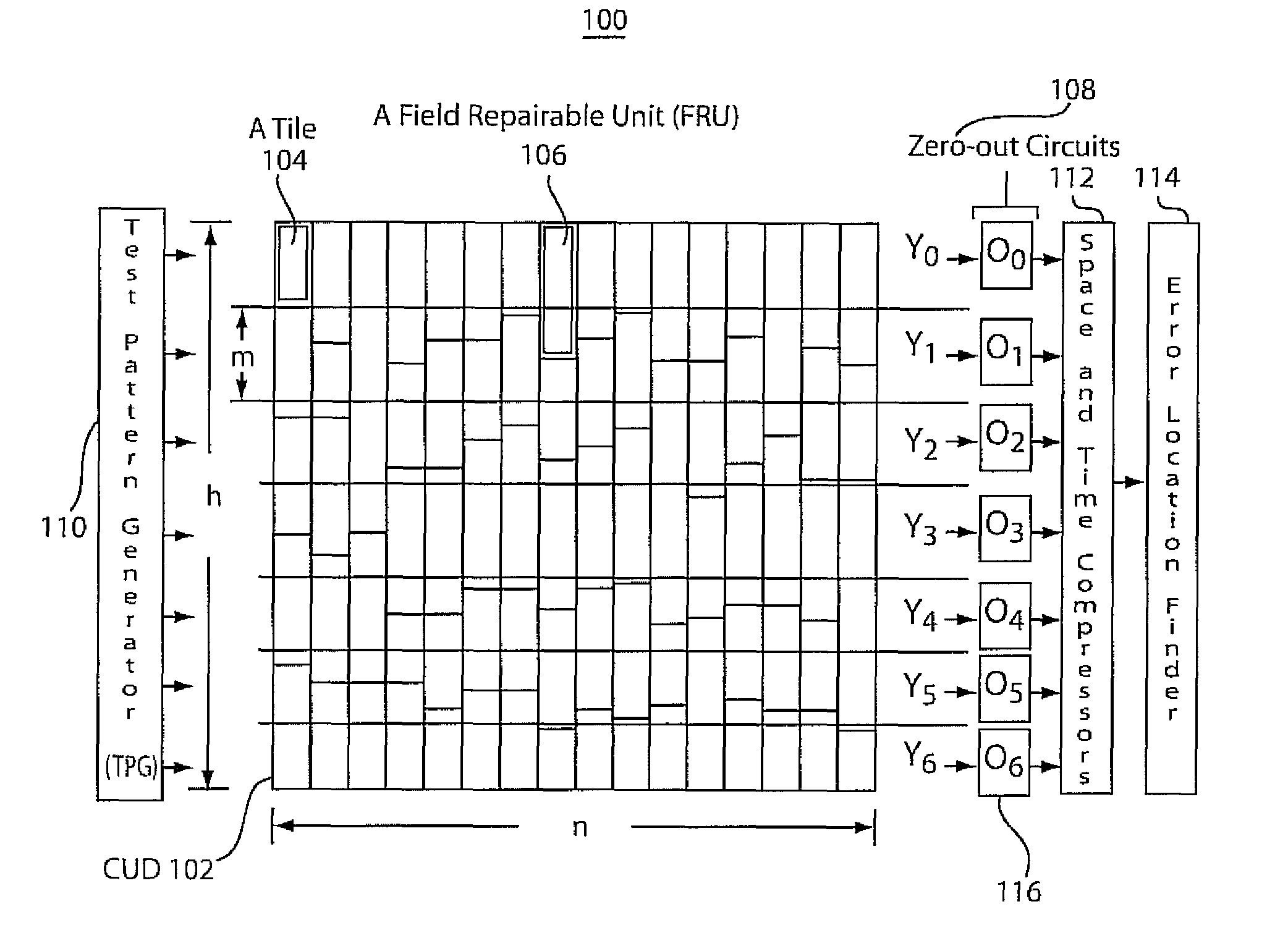
[0023]As noted above, most current testing using BISR is performed during manufacturing of circuits rather than in the field. If repairs are performed in the field as well as at manufacturing test sites, testing costs may be significantly reduced, as high reliability will be maintained even with less perfect screening. While the cost of testing transistors has been relatively constant, the cost of manufacturing a transistor has been significantly reduced as a result of persistent scaling. Hence, it would be economical to use some silicon area for field repair capability to reduce test cost. Implementing self-repair for random logics in regular application-specific integrated circuit (ASIC) devices, which have no regularity and are not field-reconfigurable, is much more difficult.

[0024]To repair defective parts by BISR, defective parts should be located through a self-diagnosis process. This includes comparing responses of the circuit under diagnosis (CUD) with responses of a defect ...


PUM


Abstract

According to exemplary methods and systems of the present principles, the location of defective field repairable units (FRUS) of a circuit that have varying sizes or varying numbers of scan cells may be identified by employing tiles including scan cells from different FRUS. A set of test patterns may be scanned through the scan cells such that cells belonging to FRUs within a tile may be concealed while analyzing the response of scan cells in the tile contributed by a different FRU. Further, defective tiles are discoverable at any tile location and in any quantity within a maximal capacity using a compressed signature. In addition, signature registers that process data at a rate that is faster than the scan shift rate of the circuit may be employed during compression to multiply a circuit response by a plurality of components of a compression matrix during one scan shift cycle.

Description

RELATED APPLICATION INFORMATION[0001]This application claims priority to provisional application Ser. No. 61 / 113,284 filed on Nov. 11, 2008 incorporated herein by reference.BACKGROUND[0002]1. Technical Field[0003]The present invention generally relates to diagnosing a circuit, and more particularly, to systems and methods for locating defective components within a circuit.[0004]2. Description of the Related Art[0005]Aggressive scaling of complementary metal-oxide-semiconductor (CMOS) technology has significantly improved performance and reduced the manufacturing cost of chips. However, despite these improvements, increased scaling may detrimentally affect chip reliability due to elevated chip temperature resulting from increased power density and leakage current. In addition, scaling has a significant impact on hard fault rates. Leakage current stemming from scaling reduces the reliability of traditional reliability circuit screening methods such as burn-in and IDD, testing. Current...

Claims


Application Information

Patent Timeline
Patent Type & Authority Patents(United States)
IPC IPC(8): G01R31/00
CPCG01R31/318547
Inventor WANG, SEONGMOONTANG, XIANGYU
Owner NEC CORP
Why Eureka
Try Eureka