Graphite crucible for growing large-size silicon carbide single crystal by physical vapor deposition method and application thereof

A technology of physical vapor deposition and silicon carbide single crystal, which is applied in the direction of single crystal growth, single crystal growth, crystal growth, etc., can solve problems such as the difficulty of growing silicon carbide single crystal materials, achieve convexity reduction, reduce production costs, crystal The effect of improving the type stability rate

Inactive Publication Date: 2012-07-04
SICC CO LTD
View PDF6 Cites 38 Cited by
  • Summary
  • Abstract
  • Description
  • Claims
  • Application Information

AI Technical Summary

Problems solved by technology

[0003] The growth of silicon carbide single crystal material is relatively difficult. According to theoretical analysis, if the SiC single crystal is grown by pulling method from the stoichiometric melt, the conditions...

Method used


Image

  • Graphite crucible for growing large-size silicon carbide single crystal by physical vapor deposition method and application thereof
  • Graphite crucible for growing large-size silicon carbide single crystal by physical vapor deposition method and application thereof
  • Graphite crucible for growing large-size silicon carbide single crystal by physical vapor deposition method and application thereof

Examples


Embodiment 1

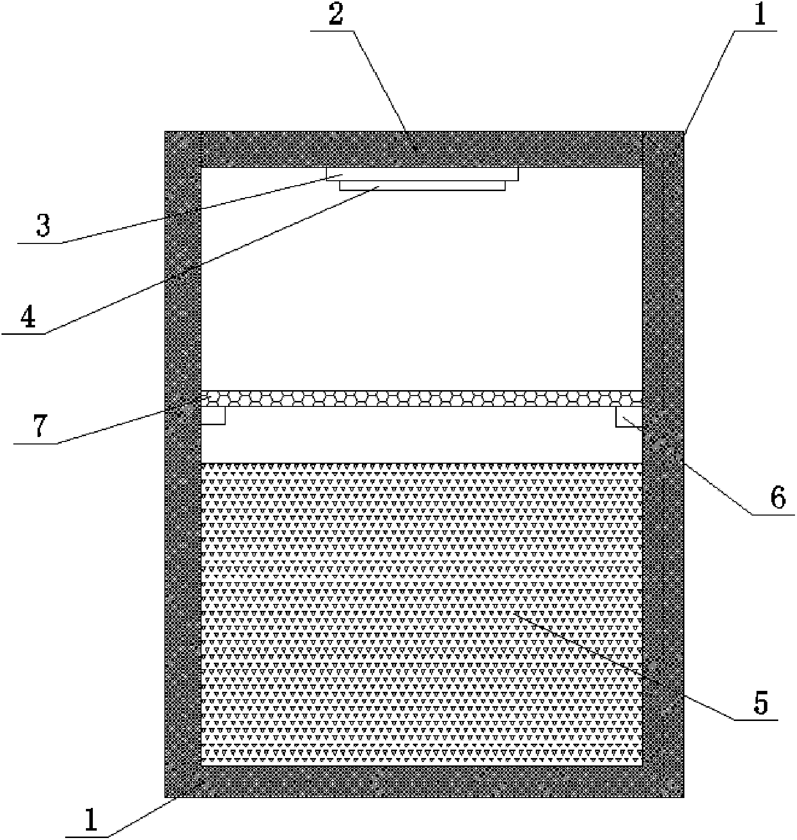
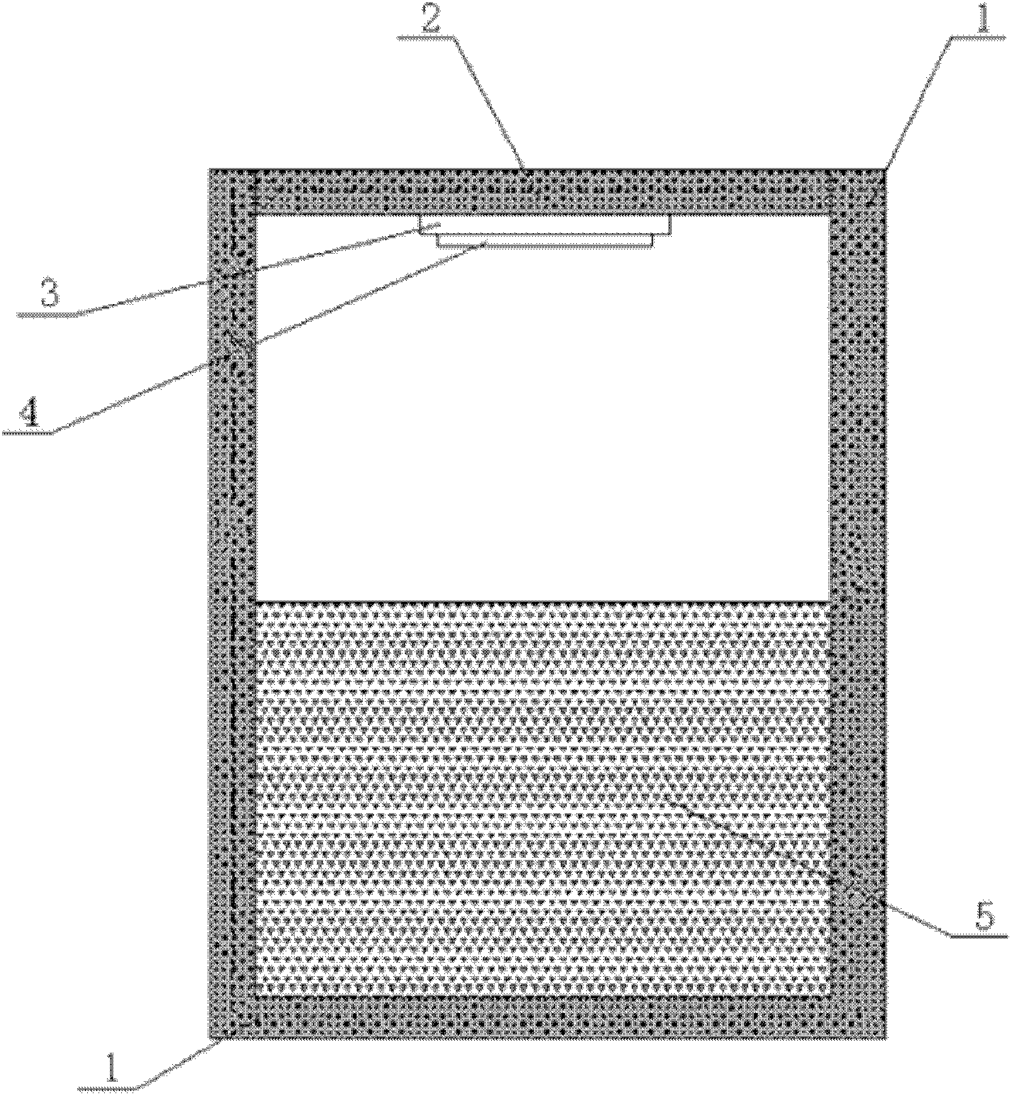
[0030] Such as figure 1 shown. A graphite crucible for growing large-size silicon carbide single crystals by physical vapor deposition, comprising a crucible barrel 1 and an upper cover 2 for containing silicon carbide raw materials, and an upper inner wall of the crucible barrel 1 and an outer wall of the upper cover 2. screw thread, the upper cover 2 and the crucible barrel 1 are connected by threads; the inner wall of the crucible barrel 1 is provided with a positioning block 6 for placing a porous graphite plate, and the positioning block 6 is along the inner wall of the crucible barrel for a week Set in a circular shape; a porous graphite plate 7 is placed on the positioning block 6, and the outer diameter of the porous graphite plate 7 should adapt to the inner diameter of the crucible barrel 1; the material of the crucible barrel 1 and the upper cover 2 is high Density graphite, the density of described high-density graphite is: 1.6g / cm 3 . The material of described ...

Embodiment 2

[0032] A method for producing silicon carbide single crystals using the graphite crucible described in Example 1, comprising adding silicon carbide raw materials into the crucible barrel 1, the distance between the upper surface of the silicon carbide raw material and the lower surface of the porous graphite plate 7 The thickness is 10mm; the seed crystal base and the seed crystal are arranged on the lower surface of the upper cover, the upper cover is connected to the crucible barrel through threads and covered, and a silicon carbide single crystal is prepared by physical vapor deposition. The physical vapor deposition method for preparing silicon carbide single crystals is a prior art.

[0033] Using the graphite crucible described in Example 1 and the method described in Example 2, 50 furnaces of 3-inch 4H-SiC single crystals were grown. The results are listed in Table 1.

Embodiment 3

[0034] Embodiment 3, the graphite crucible as described in embodiment 1, its difference is:

[0035] The positioning block 6 includes a plurality of raised blocks arranged along the inner wall of the crucible barrel; the density of the high-density graphite is 1.7g / cm 3 . The density of described low-density porous graphite is 0.5g / cm 3 , the porosity range of the porous graphite plate is 60%; the thickness of the porous graphite plate is 15mm. The inner diameter of the crucible barrel is 200mm; the height of the crucible barrel is 450mm.


PUM

PropertyMeasurementUnit
Densityaaaaaaaaaa
Densityaaaaaaaaaa
Thicknessaaaaaaaaaa

Abstract

The invention relates to a graphite crucible for growing large-size silicon carbide single crystal by a physical vapor deposition method. The graphite crucible comprises a crucible barrel for holding a silicon carbide raw material, and an upper cover, wherein mutually screwed threads are arranged on the inner wall of the crucible barrel and the outer wall of the upper cover, and the upper cover is in threaded connection with the crucible barrel; a positioning block for placing of a porous graphite plate is arranged on the inner wall of the crucible barrel; and the porous graphite plate is placed on the positioning block, and the outside diameter of the porous graphite plate is in correspondence with the inside diameter of the crucible barrel. According to the invention, the influence of carbonization of the silicon carbide raw material on the crystal growth is effectively avoided, and the crystal growth stability and success rate are improved.

Description

technical field [0001] The invention relates to a graphite crucible for growing a large-size silicon carbide single crystal by a physical vapor deposition method and an application thereof, belonging to the technical field of single crystal growth. Background technique [0002] Silicon carbide (SiC) single crystal material is a representative of the third generation of wide bandgap semiconductor materials, with properties such as wide bandgap, high thermal conductivity, high electron saturation migration rate, high breakdown electric field, etc., and the first generation represented by silicon Compared with the second-generation semiconductor materials represented by GaAs, semiconductor materials have obvious advantages, and are considered to be ideal semiconductor materials for manufacturing optoelectronic devices, high-frequency high-power devices and high-temperature electronic devices. It is widely used in white light lighting, optical storage, screen display, aerospace,...

Claims


Application Information

Patent Timeline
IPC IPC(8): C30B23/00C30B29/36
Inventor 高玉强胡小波郝霄鹏
Owner SICC CO LTD
Why Eureka
Try Eureka