Uniformity compensation device applied to large field-of-view montage illumination

A compensation device and a uniformity technology, applied in the field of large-scale integrated circuit manufacturing, can solve the problem that the uniformity of the unit illumination field of view cannot be guaranteed while meeting the requirements, etc., and achieve the effects of good illumination uniformity and high illumination uniformity

Active Publication Date: 2012-07-04
SHANGHAI MICRO ELECTRONICS EQUIP (GRP) CO LTD
View PDF6 Cites 4 Cited by
  • Summary
  • Abstract
  • Description
  • Claims
  • Application Information

AI Technical Summary

Problems solved by technology

Even if there are quartz rods and microlens arrays for uniform light after light splitting, according to the actual installation experi

Method used


Image

  • Uniformity compensation device applied to large field-of-view montage illumination
  • Uniformity compensation device applied to large field-of-view montage illumination
  • Uniformity compensation device applied to large field-of-view montage illumination

Examples


Example Embodiment

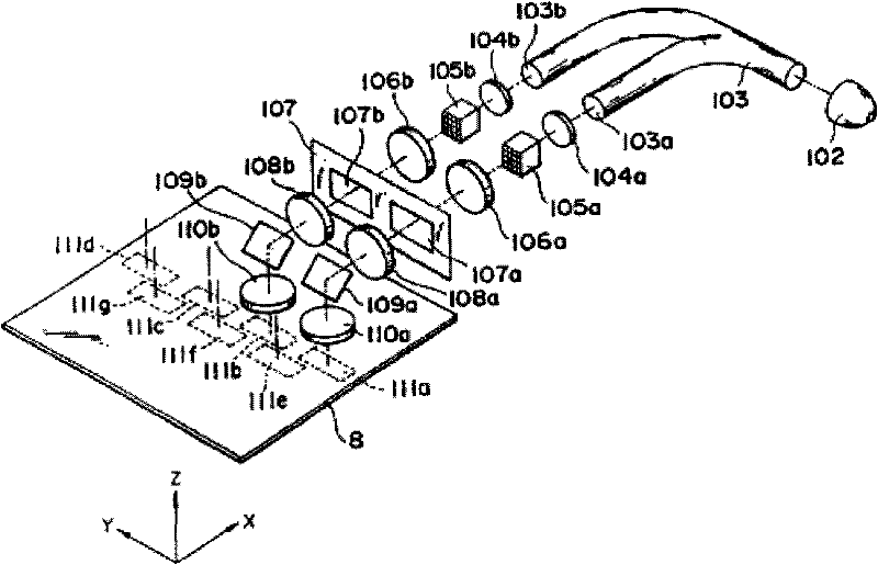
[0030] Such as Figure 4 Shown is the first embodiment of the uniformity compensation device for large field of view splicing illumination provided by the present invention, which uses a quartz rod or a microlens array to homogenize light before entering the light splitting fiber. In this implementation, the ultraviolet light emitted by the mercury lamp light source 1 is condensed by the ellipsoidal reflector 2 in sequence, and the micro lens array 3 and the quartz rod 4 are uniformly modulated. The uniformly modulated ultraviolet light enters the light splitting fiber 5 and is divided into at least two paths. A detector (not shown in the figure) is placed at the light exit of the relay lens 7 to obtain the substrate illumination uniformity signal, which is transmitted to the feedback controller 6, and the position of the mercury lamp is adjusted according to the signal.

[0031] The uniformity compensation device includes a mercury lamp light source 1, an ellipsoidal reflector 2...


PUM

PropertyMeasurementUnit
Diameteraaaaaaaaaa

Abstract

The invention provides a uniformity compensation device applied to large field-of-view montage illumination, which sequentially comprises a light source, a light distribution structure with at least two light outlets and relay lenses with the number of optical fiber light outlets to be identical along the light transmission direction. The uniformity compensation device is characterized by further comprising a light evening optical element and a feedback controller. Light emitted from the light source passes through the light evening optical element, the light distribution structure and the relay lenses to obtain a uniform illumination field of view on a substrate. The feedback controller can adjust positions and/or angles of a mercury lamp according to uniformity signals of the substrate.

Description

technical field [0001] The invention relates to the technical field of large-scale integrated circuit manufacturing, in particular to a uniformity compensation device for splicing illumination with a large field of view. Background technique [0002] TFT is the abbreviation of Thin Film Transistor (Thin Film Field Effect Transistor), which is a large-scale semiconductor full integrated circuit manufacturing technology using new materials and new processes. TFT is formed on non-single wafers such as glass or plastic substrates (of course, it can also be on wafers) through sputtering and chemical deposition processes to form various films necessary for manufacturing circuits, and to manufacture large-scale semiconductor integrated circuits (LSIC) through film processing. . With the development of related electronic consumer products, the size of TFT is required to be larger and more integrated units, it is difficult for a single lighting system to meet the requirements of TFT...

Claims


Application Information

Patent Timeline
IPC IPC(8): G03F7/20
Inventor 张祥翔
Owner SHANGHAI MICRO ELECTRONICS EQUIP (GRP) CO LTD
Why Eureka
Try Eureka