Photoetching method
A technology of lithography and photoresist, applied in the field of lithography, can solve problems such as high cost and affecting production progress, and achieve the effect of avoiding diffusion
- Summary
- Abstract
- Description
- Claims
- Application Information
AI Technical Summary
Problems solved by technology
Method used
Image

Examples
Embodiment Construction
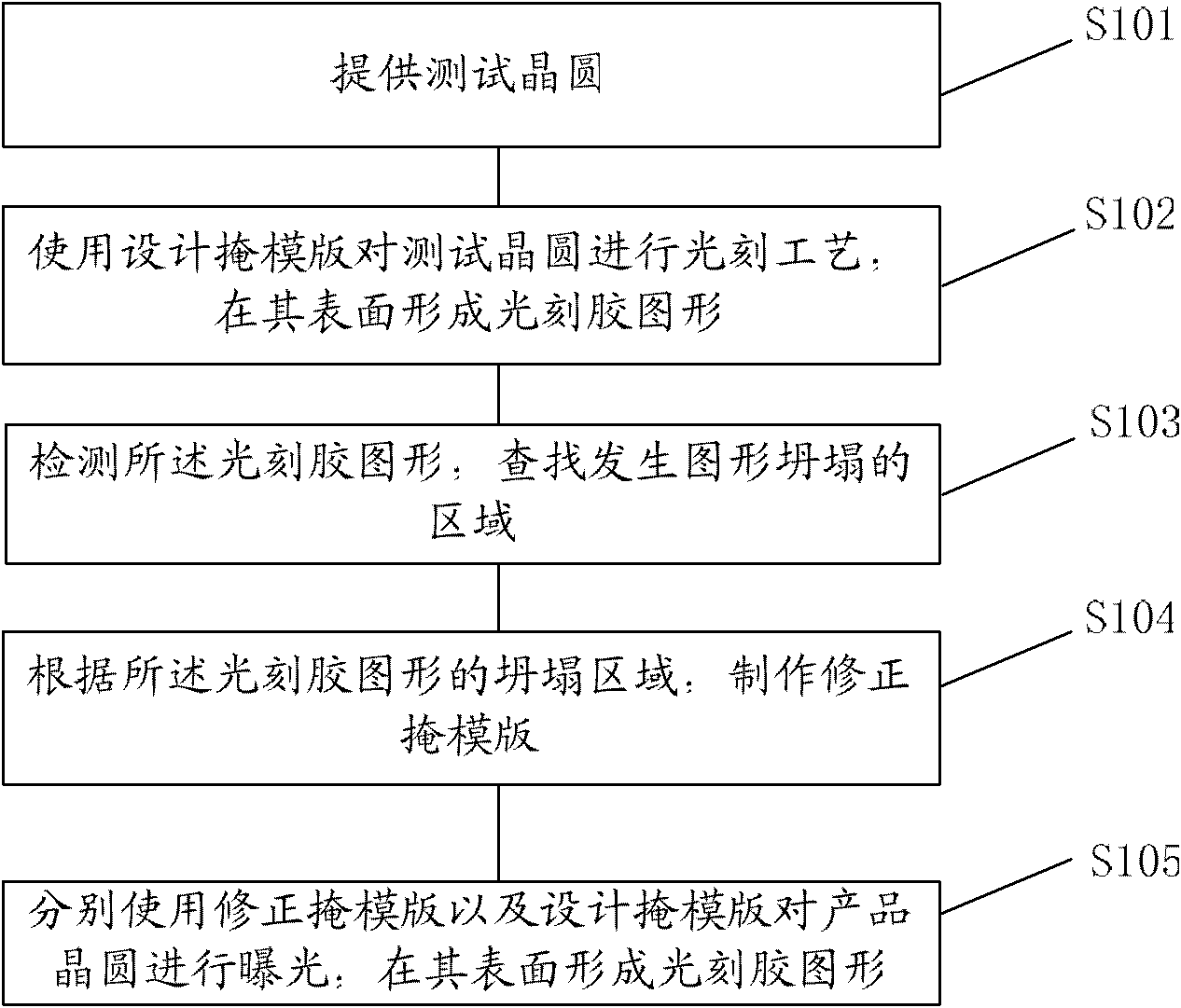
[0025] In the existing photolithography process, when the photoresist pattern on the wafer surface collapses due to layout design problems, the photoresist pattern can only be re-made and the unqualified pattern on the layout can be corrected. Therefore, the cost is higher and the production schedule is affected.
[0026] In an actual production process, one wafer is used to manufacture multiple chips, so the wafer is divided into multiple repeated chip regions. If the photoresist pattern collapses due to the design problem of the test pattern on the reticle, the pattern in the collapsed area does not have any impact on the chip function; even if the photoresist pattern is caused by the design problem of the device pattern on the reticle The collapse of the glue pattern also affects only a limited number of chips. Assuming that the above-mentioned area where the pattern collapse occurs is shielded, the rest of the wafer can still perform normal photolithography processes.
...
PUM
 Abstract
Description
Claims
Application Information
 - R&D
- Intellectual Property
- Life Sciences
- Materials
- Tech Scout
- Unparalleled Data Quality
- Higher Quality Content
- 60% Fewer Hallucinations
Browse by: Latest US Patents, China's latest patents, Technical Efficacy Thesaurus, Application Domain, Technology Topic, Popular Technical Reports.
© 2025 PatSnap. All rights reserved.Legal|Privacy policy|Modern Slavery Act Transparency Statement|Sitemap|About US| Contact US: help@patsnap.com