Measuring system and photoetching device using same

A measurement system and grating technology, applied in the field of photolithography, can solve the problems of reducing production efficiency and increasing manufacturing costs, and achieve the effect of improving production efficiency and reducing equipment manufacturing costs

Active Publication Date: 2012-07-04
SHANGHAI MICRO ELECTRONICS EQUIP (GRP) CO LTD
View PDF9 Cites 29 Cited by
  • Summary
  • Abstract
  • Description
  • Claims
  • Application Information

AI Technical Summary

Problems solved by technology

[0011] The existing lithography equipment uses two different sets of equipment to realize the functions of silicon wafe

Method used


Image

  • Measuring system and photoetching device using same
  • Measuring system and photoetching device using same
  • Measuring system and photoetching device using same

Examples


Embodiment Construction

[0051] In the following, preferred embodiments according to the present invention will be described in detail with reference to the accompanying drawings. For the convenience of describing and highlighting the present invention, relevant components existing in the prior art are omitted from the drawings, and the description of these known components will be omitted.

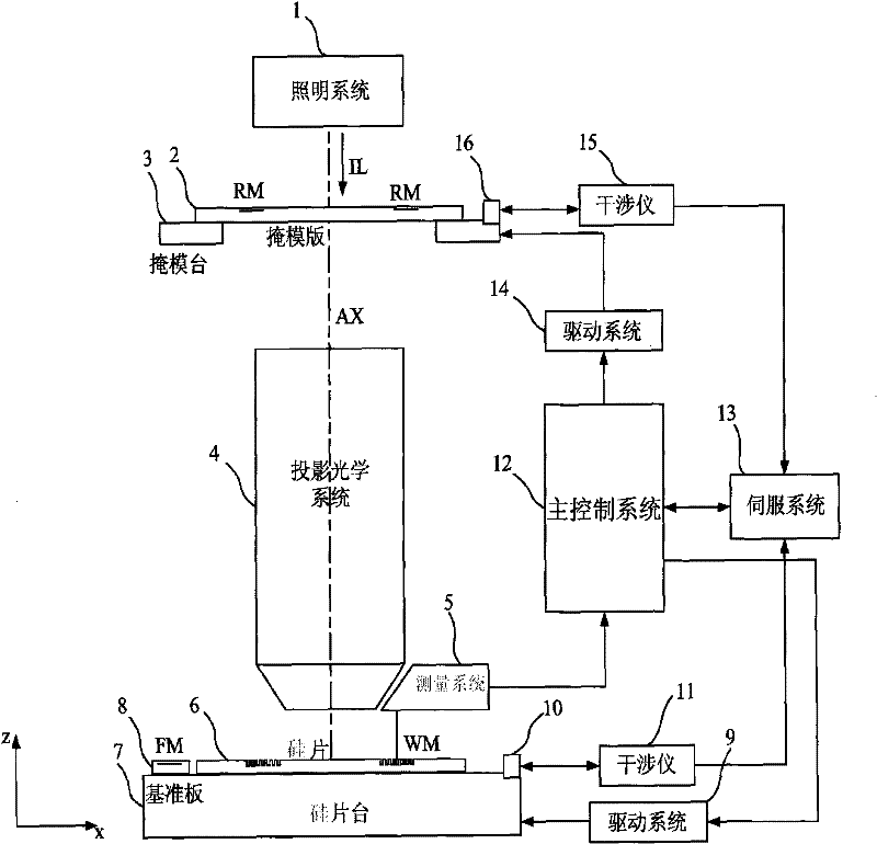
[0052] figure 1 Shown is a schematic structural view of a lithographic apparatus according to the present invention. The lithography apparatus comprises: an illumination system 1 for providing an exposure beam; a mask holder and a mask table 3 for supporting a reticle 2 with a mask pattern and an alignment mark RM having a periodic structure on the reticle 2 ; be used for projecting the mask pattern on the reticle 2 to the substrate (in this embodiment, the substrate is a silicon wafer as an example for illustration, but not to limit the present invention) 6 projection optical system 4; On the silicon wafer hol...


PUM


Abstract

The invention discloses a measuring system which comprises a light source module, an illuminating module, an imaging module and a detecting module arranged in sequence along the light propagation direction, wherein the light source module is used for emitting a light beam; after the light beam enters the illuminating module, an illuminating beam is emitted to illuminate a mark on the surface of a substrate, then after the illuminating beam is reflected and diffracted by the mark, emergent light with multiple diffraction orders are formed; the detecting module comprises a detecting grating and a light intensity detector, the light with multiple diffraction orders becomes incident light to enter into the detecting grating after passing through the imaging module, the detecting grating carries out secondary diffraction on the incident light so as to form light beams with multiple diffraction orders to form interference patterns on the light intensity detector; wherein the light with multiple diffraction orders is subjected to phase modulation through moving the substrate or the detecting grating so as to obtain the information of phase difference of the light with multiple diffraction orders, and then according to the information of phase difference, the three-dimensional position information of the substrate is obtained, thereby realizing alignment, focusing and leveling measurement on the substrate.

Description

technical field [0001] The invention relates to the field of lithography, in particular to a measurement system for silicon wafer alignment and focus adjustment and leveling in lithography equipment. Background technique [0002] In the prior art, the patterns formed on various masks are illuminated with exposure light, and the exposure device that copies the aforementioned patterns onto substrates such as wafers and glass substrates coated with photoresist through an imaging optical system is openly known. The current lithography equipment is mainly divided into two categories, one is stepping lithography equipment, the mask pattern is exposed and imaged on one exposure area of ​​the silicon wafer, and then the silicon wafer moves relative to the mask to move the next exposure area to Underneath the mask pattern and the projection objective, the mask pattern is again exposed on another exposed area of ​​the wafer, and the process is repeated until all exposed areas on the ...

Claims


Application Information

Patent Timeline
IPC IPC(8): G03F9/00G03F7/20G01J9/02
Inventor 王帆马明英
Owner SHANGHAI MICRO ELECTRONICS EQUIP (GRP) CO LTD
Why Eureka
Try Eureka