
Memory interface access control method and device

A memory access and interface control technology, applied in program control design, instrumentation, memory address/allocation/relocation, etc., can solve the problem of low effective bandwidth of DDRX, and achieve the goal of improving overall performance, increasing throughput bandwidth, and improving access efficiency. Effect

Active Publication Date: 2012-07-04
ZTE CORP
View PDF4 Cites 15 Cited by
  • Summary
  • Abstract
  • Description
  • Claims
  • Application Information

AI Technical Summary

Problems solved by technology

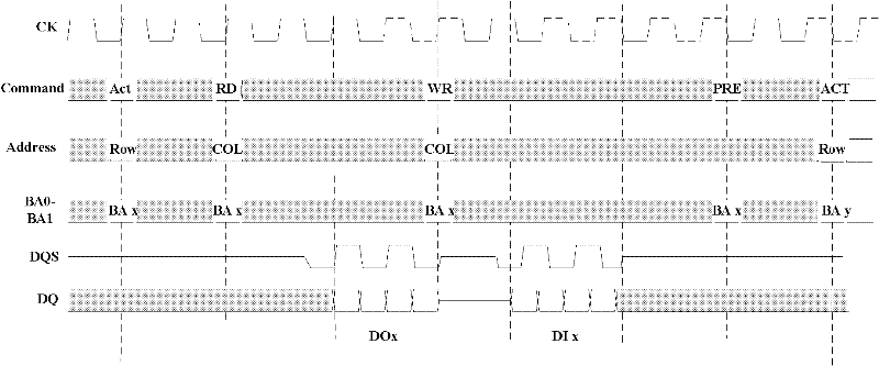
Therefore, in existing applications, the effective bandwidth of DDRX is very low. No matter how high the rate of the interface is, the actual utilization rate of bandwidth resources is only about one-tenth.

Method used


Image

  • Memory interface access control method and device
  • Memory interface access control method and device
  • Memory interface access control method and device

Examples


Embodiment 1

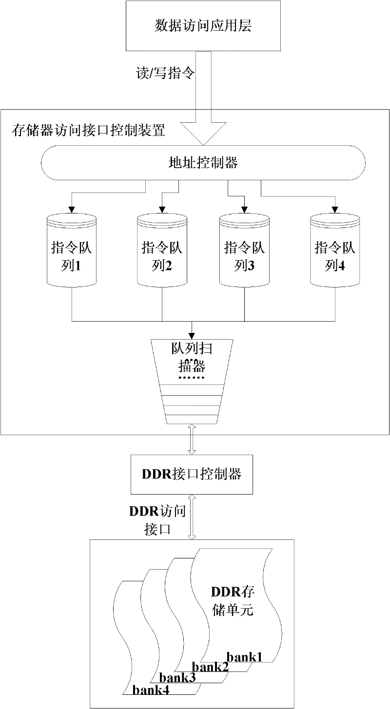
[0058] The memory interface access control device provided by the embodiment of the present invention is set between the data storage application layer and the DDRX interface controller, the read and write instructions are sent from the data storage application layer as required, and the DDRX interface controls the access interface that converts the read and write instructions into DDRX . After the device of the invention processes the read and write instructions issued by the data storage application layer, the processed read and write instructions are sent to the DDRX interface controller.

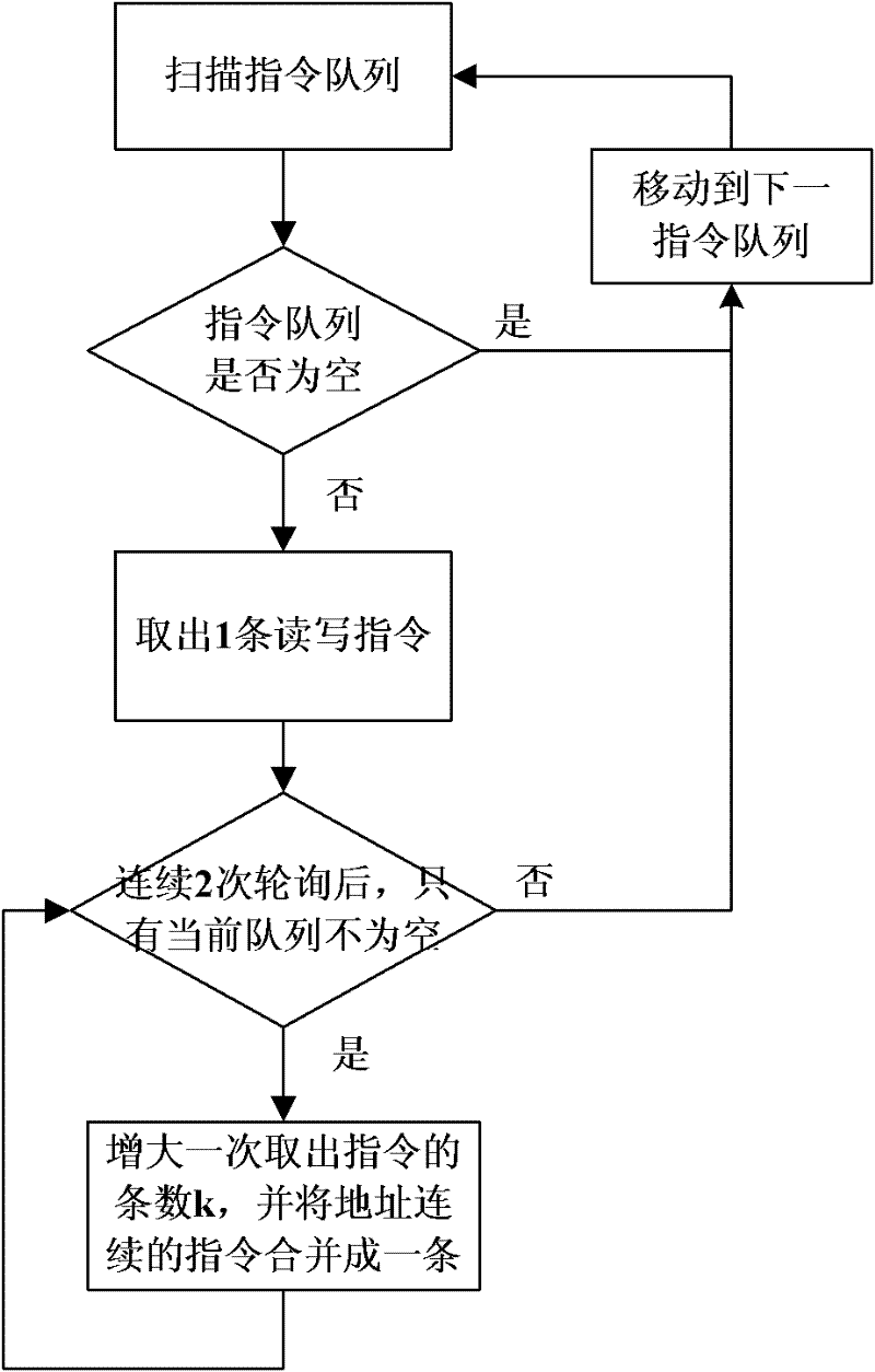
[0059] Such as figure 2 As shown, the memory interface access control device according to the embodiment of the present invention mainly includes three parts: an address controller, an instruction queue, and a queue scanner.

[0060] The address controller is mainly used to remap the addresses in the read and write instructions sent by the data storage application layer. The specific ...

Embodiment 2

[0078] Figure 4 A DDRII device is shown as an example to describe an embodiment of this patent. The storage access of the application layer initiates read and write requests through three sets of signals, including: write command signal composed of wr_en, cmd, wr_data, wr_addr; read command signal composed of rd_en, cmd, rd_addr; read data valid indication composed of rd_data and data_valid Signal. The write command signal and the read command signal pass through the corresponding wr_cmd_fifo and rd_cmd_fifo to guide the access command flow of the application layer, which is convenient for the command controller to schedule.

[0079] The access address processed by cmd_fifo needs to be mapped. Its function is to map the address table in the application layer to different BANKs in the DDRII memory, so that the accessed data is evenly mapped in 8 different BANKs. The mapped address and the corresponding command are combined into an access command field, which is imported into...


PUM


Abstract

The invention discloses a memory interface access control method and device. The device comprises an address controller, an instruction queue and an instruction queue scanner which are sequentially connected, wherein the address controller is connected with a data storage application layer, the instruction queue scanner is connected with an interface controller of a memory, the address controller is used for respectively mapping an instruction sent by the data storage application layer into different spaces of the memory and sending read write instructions of different spaces into corresponding instruction queues; each instruction queue is used for caching received read write instructions; and the queue scanner is used for sequentially reading the read write instructions from each instruction queue and sending the read write instructions into the interface controller of the memory. By adopting the memory interface access control method and device disclosed by the invention, throughput width of a DDRX (discontinuous dynamic recrystallization) memory can be effectively improved, the same effect can be realized on a read operation and a write operation, and access efficiency of the memory can be improved, thus overall performance of equipment is enhanced.

Description

technical field [0001] The present invention relates to the technical field of DDR (Double Data Rate, double-rate synchronous dynamic random access memory), and more specifically, to a memory interface access method and device. Background technique [0002] DDRX type memory is widely used in various communication devices, including DDR, DDRII and DDRIII, which use double-rate data bus memory. Compared with SSRAM (Synchronous Static Random Access Memory, Synchronous Static Random Access Memory), it stores High density (up to 1Gbit for a single particle), high interface rate (up to 1.333Ghz), low cost, and other advantages make it one of the most important devices in memory. [0003] In order to achieve the above-mentioned excellent characteristics, a lot of price must be paid in the design of the device. In order to achieve the index of larger storage capacity on a single chip, it is necessary to use as few transistors as possible in each storage unit (SSRAM requires at leas...

Claims


Application Information

Patent Timeline
Patent Type & Authority Applications(China)
IPC IPC(8): G06F13/16G06F12/02
CPCG06F9/00G06F13/16G06F12/02G06F13/1668
Inventor 黄科
Owner ZTE CORP
Learn More