
Method for forming multistage deep step

A step and depth technology, which is applied in the field of forming multi-level deep steps, can solve the problems of step limitation, inability to develop, and deformation of photolithographic graphics, etc., and achieve the effect of solving the limitation of step length and steps

Inactive Publication Date: 2012-07-04
ADVANCED SEMICON MFG CO LTD
View PDF2 Cites 7 Cited by
  • Summary
  • Abstract
  • Description
  • Claims
  • Application Information

AI Technical Summary

Problems solved by technology

However, if the steps are too deep (several microns), not only a very thick photoresist is required for the photolithography of the next layer of steps, but also the photoresist cannot be thrown evenly, resulting in deformation of the photolithographic pattern or even failure to develop and many other issues
Therefore, the steps are restricted

Method used


Image

  • Method for forming multistage deep step
  • Method for forming multistage deep step
  • Method for forming multistage deep step

Examples


Embodiment Construction

[0029] The present invention will be described in further detail below in conjunction with accompanying drawing:

[0030] In the following description, numerous specific details are set forth in order to provide a thorough understanding of the present invention. However, the present invention can be implemented in many other ways different from those described here, and those skilled in the art can make similar extensions without violating the connotation of the present invention, so the present invention is not limited by the specific implementations disclosed below.

[0031] Secondly, the present invention is described in detail using schematic diagrams. When describing the embodiments of the present invention in detail, for the convenience of explanation, the cross-sectional view showing the device structure will not be partially enlarged according to the general scale, and the schematic diagram is only an example, and it should not be limited here. The protection scope of ...


PUM


Abstract

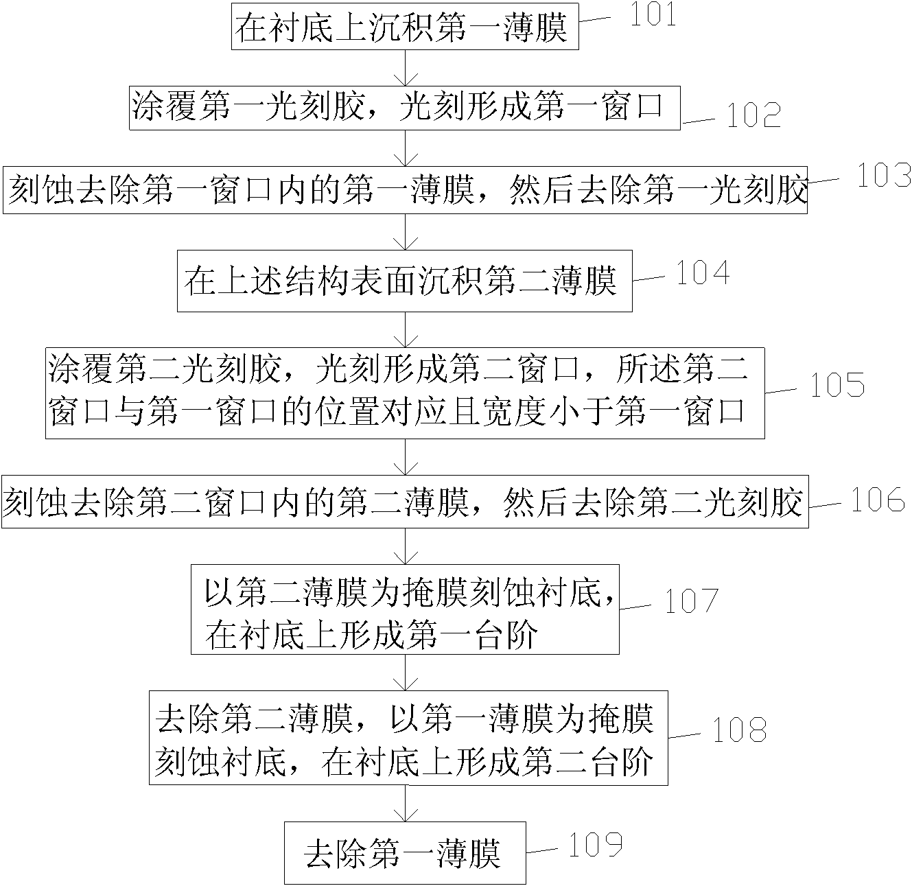
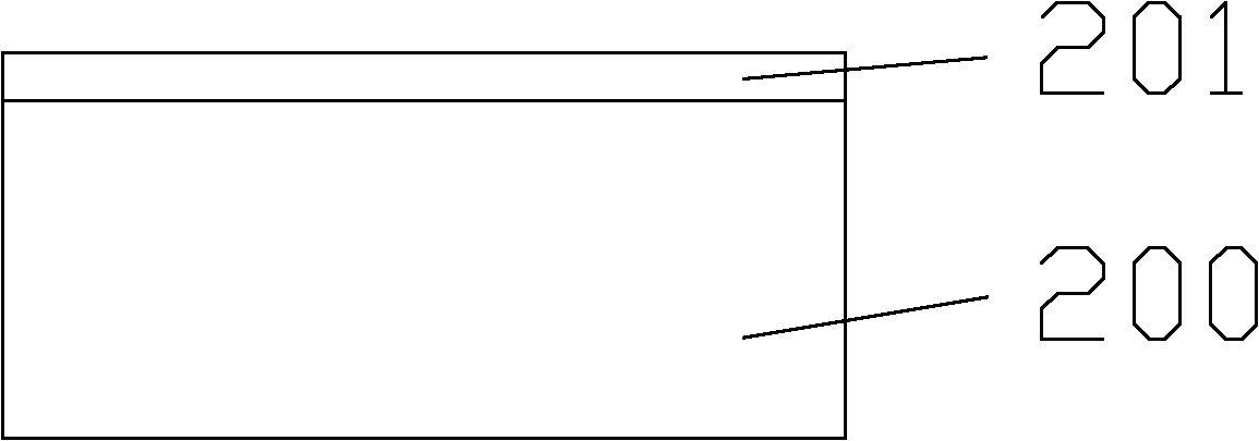
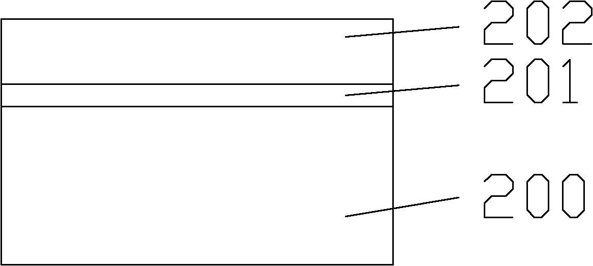
The invention relates to a method for forming a multistage deep step, which comprises the following steps of: depositing a first film on a substrate; coating first photoresist, and photoetching the first photoresist to form a first wind; removing the first film within the first window through etching, and then removing the first photoresist; depositing a second film on the surface of the structure; coating second photoresist; and etching the second photoresist to form a second window, wherein the position of the second window is corresponding to that of the first window, and the width of the second window is smaller than that of the first window; removing the second film in the second window through etching, and then removing the second photoresist; etching the substrate by using the second film as a mask to form a first step on the substrate; removing the second film, and etching the substrate by using the first film as a mask to form a second step on the substrate; and removing the first film. In the method, multiple films are respectively used as etching baffle layers for each step, the problem of limited step length and steps is solved, and a multistage deep step structure of a single material is made.

Description

technical field [0001] The invention relates to the technical field of semiconductors, in particular to a method for forming multi-level deep steps. Background technique [0002] In the manufacturing process of some semiconductor devices, it is necessary to form several deep (micron-scale) steps on the substrate to form a specific structure and achieve certain properties. This structure is commonly used in devices such as MEMS. [0003] For the realization of this multi-level step structure, the following two methods can usually be adopted: one is to deposit multi-layer films on the substrate, and obtain step structures of various materials through etching and patterning of the films; the other is It is to directly etch the substrate to obtain a multi-level stepped structure of a single material. [0004] If the first method is adopted, that is, to deposit multi-layer thin films, and to form steps of various materials upward, when the step length is large (greater than 1mm...

Claims


Application Information

Patent Timeline
Patent Type & Authority Applications(China)
IPC IPC(8): H01L21/02
Inventor 陈健张艳红张挺
Owner ADVANCED SEMICON MFG CO LTD
Learn More