Manufacturing method of metal gate electrode

A technology of metal gate and manufacturing method, which is applied in semiconductor/solid-state device manufacturing, electrical components, semiconductor devices, etc., can solve the problems of sidewall layer collapse, unbalanced pressure, affecting the shape of metal gate, etc.

Active Publication Date: 2012-07-04
SEMICON MFG INT (SHANGHAI) CORP +1
View PDF4 Cites 3 Cited by
  • Summary
  • Abstract
  • Description
  • Claims
  • Application Information

AI Technical Summary

Problems solved by technology

[0023] In the above process, if Figure 7 As shown in , the shape of the fabricated metal gate is not the shape of the replacement gate because, in Image 6 In the process of etching the replacement gate, the pressure applied to the upper half of the sidewall layer is different from the pressure applied to the lower half of the sidewall layer, and the pressure applied to the upper half of the sidewall layer There is no interlayer dielectric layer, so the pressure is relatively large, and the lower half of the side wall layer has an interlayer dielectric layer, so the pressure is relatively small. Due to the unbalanced pressure, the side wall layer will collapse, thereby Changes the shape of the replacement gate trench formed by the sidewall layer, which ultimately affects the shape of the metal gate

Method used


Image

  • Manufacturing method of metal gate electrode
  • Manufacturing method of metal gate electrode
  • Manufacturing method of metal gate electrode

Examples


Embodiment Construction

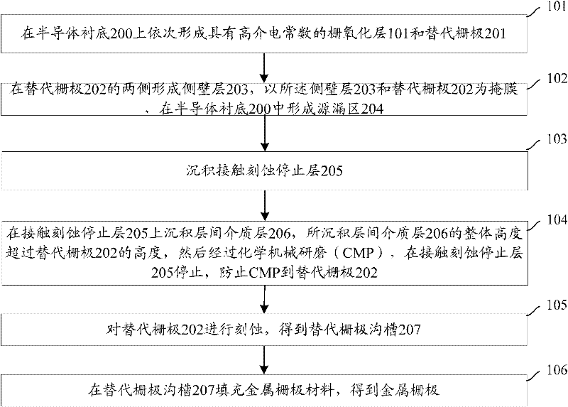
[0045] In order to make the object, technical solution and advantages of the present invention clearer, the present invention will be further described in detail below with reference to the accompanying drawings and examples.

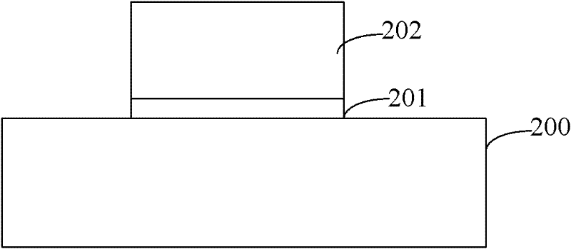
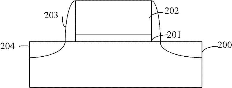
[0046] It can be seen from the prior art that the reason why the shape of the final metal gate is different from that of the replacement gate is that the shape of the replacement gate trench formed by the sidewall layer changes, so that the method of filling the replacement gate trench The shape of the metal gate fabricated by the method changes. The shape change of the replacement gate trench formed by the sidewall layer is caused by the collapse of the sidewall layer during the process of etching the replacement gate. The collapse of the sidewall layer is because various parts of the sidewall layer are etching the replacement gate. It is caused by the difference in pressure at extreme times.

[0047]Therefore, in order to eliminate the impact of the ...


PUM


Abstract

The invention discloses a manufacturing method of a metal gate electrode, which comprises the steps of: forming side wall layers at both sides of a substitution gate electrode after forming a gate oxide layer and the substitution gate electrode on a provided semiconductor substrate; taking the side wall layers and the substitution gate electrode as masking membranes to carry out ion implantation to the semiconductor substrate to form a source leakage area; depositing contact etching stop layers on the semiconductor substrate, the side wall layers and the surface of the substitution gate electrode; after depositing an interlayer medium layer on the contact etching stop layer, polishing the deposited interlayer medium layer of which the height exceeds the surface of the substitution gate electrode to the etching stop layer; after depositing a stretching layer which ensures the pressure of each part of the side wall layers identical in follow-up substitution gate electrode etching on the interlayer medium layer, polishing the stretching layer to the interlayer medium layer; and etching away the substitution gate electrode to obtain a substitution gate electrode groove, and filling a metal gate electrode in the substitution gate electrode groove. The method makes the shape of the manufactured metal gate electrode be the shape of the substitution gate electrode.

Description

technical field [0001] The invention relates to detection technology in the field of semiconductors, in particular to a method for manufacturing a metal gate. Background technique [0002] Currently, high dielectric constant insulating materials and metal gates will be used to manufacture logic circuit devices in semiconductor devices. [0003] In order to control the short channel effect, semiconductor devices with smaller feature sizes require a further increase in gate electrode capacitance. This can be achieved by continuously reducing the thickness of the gate oxide layer, but this is accompanied by an increase in gate electrode leakage current. When silicon dioxide is used as the gate oxide layer and the thickness is below 3.0nm, the leakage current becomes unbearable. The way to solve the above problems is to use high dielectric constant insulating materials to replace silicon dioxide. High dielectric constant insulating materials can be hafnium silicate, hafnium si...

Claims


Application Information

Patent Timeline
Patent Type & Authority Applications(China)
IPC IPC(8): H01L21/28H01L21/283
Inventor 鲍宇张彬
Owner SEMICON MFG INT (SHANGHAI) CORP
Why Eureka
Try Eureka