Manufacturing method of MOS (metal oxide semiconductor) device

A technology of a MOS device and a manufacturing method, which is applied in the fields of semiconductor/solid-state device manufacturing, electrical components, circuits, etc., can solve the problems of reduced control capability, consumption of single crystal silicon, etching of the semiconductor substrate 10, etc., to eliminate spacing, avoid effect of influence

Inactive Publication Date: 2012-07-04
SEMICONDUCTOR MANUFACTURING INTERNATIONAL (BEIJING) CORP
View PDF6 Cites 3 Cited by
  • Summary
  • Abstract
  • Description
  • Claims
  • Application Information

AI Technical Summary

Problems solved by technology

[0006] The prior art has the following problems: on the one hand, when etching the polysilicon layer 12 and the gate dielectric layer 11 to form the gate structure 13, it is easy to over-etch the semiconductor substrate 10; When one layer of silicon oxide film 14 is formed, the polysilicon on the gate 13 and the single crystal silicon on the semiconductor substrate 10 will be consumed; the above two factors cause a certain loss in the surface thickness of the semiconductor substrate 10, the above-mentioned Thickness loss is negligible in the manufacturing process of large feature size devices, but in small feature size devices, it will have certain problems
In a MOS device with a small feature size, the distance H will reduce the ability of the gate 13 to control the channel, resulting in an increase in the threshold voltage of the transistor, thereby affecting the electrical performance of the MOS device

Method used


Image

  • Manufacturing method of MOS (metal oxide semiconductor) device
  • Manufacturing method of MOS (metal oxide semiconductor) device
  • Manufacturing method of MOS (metal oxide semiconductor) device

Examples


Embodiment Construction

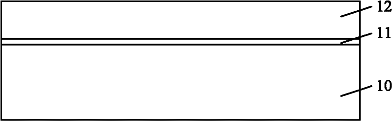
[0030] As mentioned in the background technology section, in the existing small feature size MOS device manufacturing method, due to the silicon recess phenomenon generated on the semiconductor substrate by the thermal oxidation process, a gap is formed between the bottom of the gate and the channel, and the distance between the gate and the channel The control ability of the MOS device is reduced, which in turn leads to an increase in the threshold voltage of the transistor, which affects the electrical performance of the MOS device.

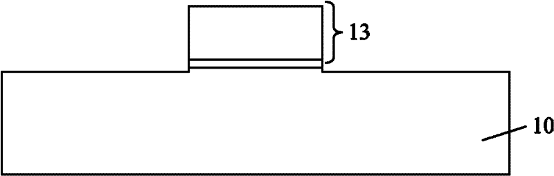
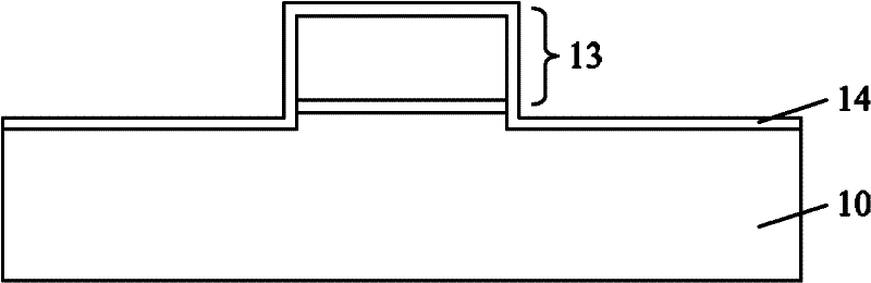
[0031] In view of the above problems, the inventors of the present invention provide a method for fabricating a MOS device. When forming the gate, the bottom of the gate is lower than the surface of the semiconductor substrate, so as to compensate for the semiconductor substrate being damaged in the gate etching process and thermal oxidation process. The thickness lost in the middle, thereby eliminating the gap between the bottom of the gate and...


PUM

PropertyMeasurementUnit
thicknessaaaaaaaaaa

Abstract

The invention provides a manufacturing method of an MOS (metal oxide semiconductor) device. The manufacturing method comprises the following steps of: providing a semiconductor substrate and forming a hard mask layer on the surface of the semiconductor substrate; etching the hard mask layer and the semiconductor substrate to form a first groove, wherein the bottom surface of the first groove is lower than the surface of the semiconductor substrate, and the height difference exists between the two; forming a gate dielectric layer on the surface of the semiconductor substrate at the bottom of the first groove; filling the first groove to form a gate electrode; removing the hard mask layer; and forming a thin film oxidation layer on the surface of the semiconductor substrate through a heat oxidation process, wherein the bottom surface of the thin film oxidation layer is higher than or flush with that of the gate dielectric layer. According to the manufacturing method disclosed by the invention, the bottom of the gate electrode is lower than the surface of the semiconductor substrate, and the height difference exists between the two; and when the thin film oxidation layer is formed by heat oxidation, the thickness loss of the semiconductor substrate is not greater than the height difference, so that a spacing interval between the bottom of the gate electrode and a channel is further eliminated and a silicon recess can be further prevented from affecting the electrical properties of the MOS device.

Description

technical field [0001] The present invention relates to the technical field of semiconductors, and more specifically, the present invention relates to a manufacturing method of a MOS device. Background technique [0002] With the rapid development of semiconductor technology, the feature size of semiconductor devices is gradually reduced, and correspondingly higher requirements are put forward for the chip manufacturing process. In a small-sized MOS device, in order to reduce the stress caused by the sidewall of silicon nitride, the sidewall of the transistor gate usually adopts a silicon oxide-silicon nitride-silicon oxide (ONO) sandwich structure. Wherein, there is lower stress and better adhesion between the gate made of silicon oxide and polysilicon, and the sidewall of the ONO can achieve better protection for the gate. For more information about the fabrication method of MOS devices with ONO sidewalls, please refer to Chinese Patent No. ZL2006101168433. Figure 1 to F...

Claims


Application Information

Patent Timeline
Patent Type & Authority Applications(China)
IPC IPC(8): H01L21/336H01L21/285H01L21/3105
Inventor 禹国宾三重野文健
Owner SEMICONDUCTOR MANUFACTURING INTERNATIONAL (BEIJING) CORP
Why Eureka
Try Eureka