Selective wave soldering equipment of PCBs (printed circuit boards)

A wave soldering and selective technology, applied in the direction of welding equipment, metal processing equipment, auxiliary equipment, etc., can solve the problems affecting the mounting components, etc., and achieve the effect of simple structure, convenient use, and easy promotion and application

Inactive Publication Date: 2012-07-04
XIAN ZHONGKEMAITE ELECTRONICS TECH EQUIP
View PDF3 Cites 6 Cited by
  • Summary
  • Abstract
  • Description
  • Claims
  • Application Information

AI Technical Summary

Problems solved by technology

[0002] With the development of electronic products, due to the constraints of various functions and conditions of use, the components on the PCB show a trend of diversification. There are all through-hole plug-in PCBs, all patch PCBs, and plug-in mixed PCBs. The current The process is that all through-hole plug-in PCBs are soldered with a wave soldering machine; all patch PCBs are soldered with a reflow soldering machine; there are two types of plug-in mixed PCBs, and the plug-in mixed components on the same side of the PCB are first soldered with a reflow soldering machine Mount the components, and then solder the plug-in components with a wave soldering machine; if the plug-in mixed components are not on the same side of the PCB, first use the reflow soldering machine to solder the mounted components, and then manually solder the plug-in components, because if you use a wave soldering machine to solder the plug-in components Mounted components will affect soldered mounted components

Method used


Image

  • Selective wave soldering equipment of PCBs (printed circuit boards)
  • Selective wave soldering equipment of PCBs (printed circuit boards)
  • Selective wave soldering equipment of PCBs (printed circuit boards)

Examples


Embodiment Construction

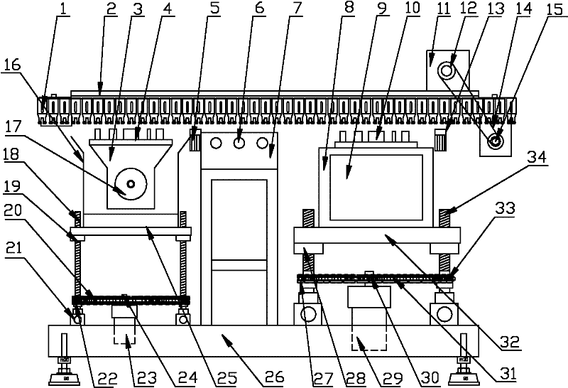
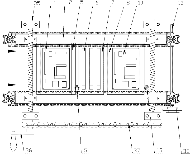
[0026] like figure 1 and figure 2 The shown PCB selective wave soldering equipment includes a guide rail 2 and a chassis 26, the guide rail 2 is provided with a chain claw 1, and a flux selective coating is installed between the chassis 26 and the guide rail 2 Components, PCB preheating components, selective wave soldering components and PCB conveying components, the flux selective coating components include foaming box 3, foaming template 4, flux box 16, foaming tube 17, flux lifting Screw mandrel 18, flux lifting nut 19, flux lifting chain 20, screw mandrel base one 21, flux lifting sprocket 22, flux lifting motor 23, motor sprocket one 24, flux lifting horizontal frame 25, all The screw base one 21 is installed on the chassis 26, the flux lifting screw 18 is installed on the chassis 26 through the screw base one 21, and the flux lifting screw 19 is installed on the flux lifting screw 18 and the flux lifting horizontal frame 25 is fixed on the flux lifting screw rod 18, t...


PUM


Abstract

The invention discloses selective wave soldering equipment of PCBs (printed circuit boards). The selective wave soldering equipment comprises a guide rail and a bottom frame, wherein the guide rail is provided with a chain claw; and a soldering flux selective-coating assembly, a PCB preheating assembly, a selective wave soldering assembly and a PCB conveying assembly are arranged between the bottom frame and the guide rail. The selective wave soldering equipment of the PCBs can realize continuous and selective wave soldering of the PCBs by intelligent control. The selective wave soldering equipment has the advantages of simple structure, is convenient to use and promote and apply.

Description

technical field [0001] The invention relates to a soldering device, in particular to a PCB selective wave soldering device. Background technique [0002] With the development of electronic products, due to the constraints of various functions and conditions of use, the components on the PCB show a trend of diversification. There are all through-hole plug-in PCBs, all patch PCBs, and plug-in mixed PCBs. The current The process is that all through-hole plug-in PCBs are soldered with a wave soldering machine; all patch PCBs are soldered with a reflow soldering machine; there are two types of plug-in mixed PCBs, and the plug-in mixed components on the same side of the PCB are first soldered with a reflow soldering machine Mount the components, and then solder the plug-in components with a wave soldering machine; if the plug-in mixed components are not on the same side of the PCB, first use the reflow soldering machine to solder the mounted components, and then manually solder th...

Claims


Application Information

Patent Timeline
Patent Type & Authority Applications(China)
IPC IPC(8): H05K3/34B23K3/00B23K3/08
Inventor 张国琦曹捷梁保华麻树波
Owner XIAN ZHONGKEMAITE ELECTRONICS TECH EQUIP
Why Eureka
Try Eureka