A wafer testing method
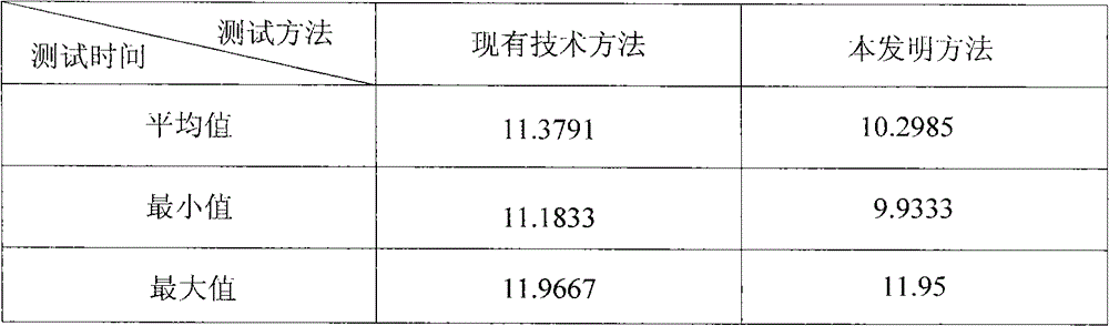
A wafer testing and wafer technology, applied in the direction of single semiconductor device testing, etc., can solve the problems of inability to adjust the testing strategy on the wafer and spend a lot of testing time, and achieve the effect of saving testing costs, saving testing time, and ensuring accuracy
- Summary
- Abstract
- Description
- Claims
- Application Information
AI Technical Summary
Problems solved by technology
Method used
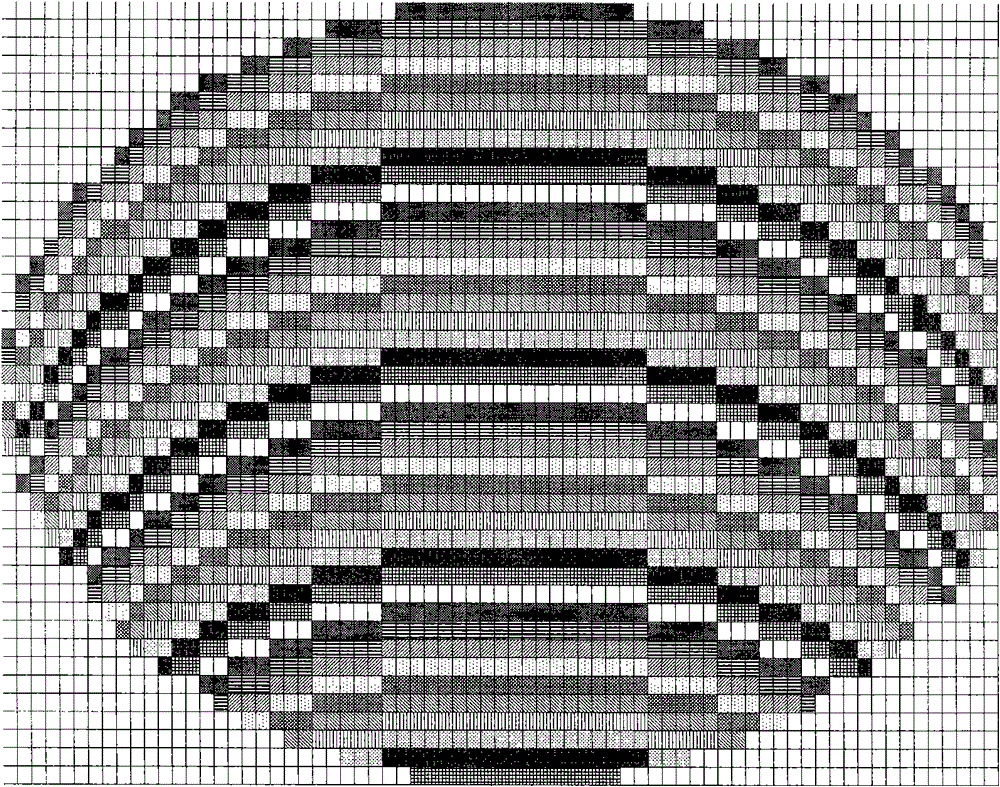
Image

Examples
Embodiment Construction
[0014] In order to make the above objects, features and advantages of the present invention more obvious and comprehensible, specific implementations of the present invention will be described in detail below.
[0015] Wafer testing method described in the present invention can utilize multiple alternatives to realize, the following is to illustrate by preferred embodiment, certainly the present invention is not limited to this specific embodiment, those of ordinary skill in the art are well known The general replacement of the above is undoubtedly covered within the protection scope of the present invention.
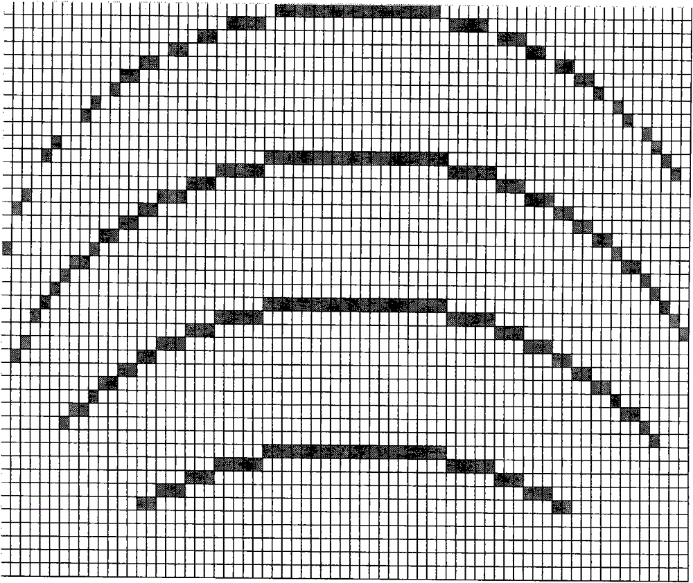
[0016] Please see figure 2 , figure 2 It is a schematic diagram of the first step of the wafer testing method of the present invention. Such as figure 2 As shown, the wafer test method of the present invention has been further improved based on the existing wafer parallel test method, comprising the following steps:
[0017] Step 1, providing a wafer to be tested...
PUM
 Abstract
Description
Claims
Application Information
 - R&D
- Intellectual Property
- Life Sciences
- Materials
- Tech Scout
- Unparalleled Data Quality
- Higher Quality Content
- 60% Fewer Hallucinations
Browse by: Latest US Patents, China's latest patents, Technical Efficacy Thesaurus, Application Domain, Technology Topic, Popular Technical Reports.
© 2025 PatSnap. All rights reserved.Legal|Privacy policy|Modern Slavery Act Transparency Statement|Sitemap|About US| Contact US: help@patsnap.com