Test device

A test device and test bench technology, applied in the directions of printed circuit testing, electronic circuit testing, etc., can solve the problems of time-consuming, damage to test terminals or circuit boards, and increased testing time, so as to reduce production costs, reduce testing time, and reduce operations. effect of steps

Inactive Publication Date: 2012-07-11
ASKEY COMP
View PDF2 Cites 3 Cited by
  • Summary
  • Abstract
  • Description
  • Claims
  • Application Information

AI Technical Summary

Problems solved by technology

However, the existing technology only uses simple fixtures to fix the wireless network card for detection, and connects the high-frequency test terminals manually. Therefore, the expensive high-frequency test terminals are often damaged due to difficult alignment, or the connection terminals or Other components are bent or damaged due to improper application of force, which increases the cost of product testing; and, in order to avoid the above-mentioned situation, the operator must carefully perform alignment insertion and extraction, which increases the test time
[0004] Existing test methods may damage the test terminals or circuit boards, and the operation is inconvenient and time-consuming, which virtually increases the cost of the product

Method used


Image

  • Test device
  • Test device
  • Test device

Examples


Embodiment Construction

[0054] In order to fully understand the purpose, features and effects of the present invention, the present invention will be described in detail with the help of the following specific examples and accompanying drawings.

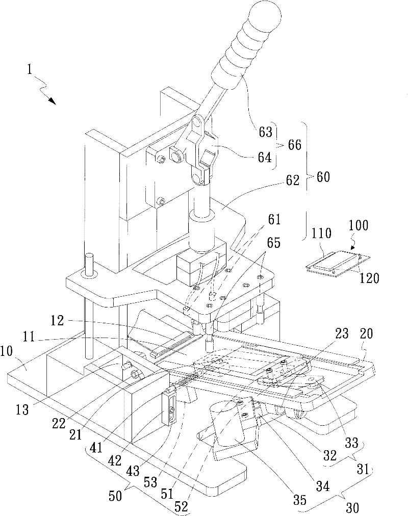
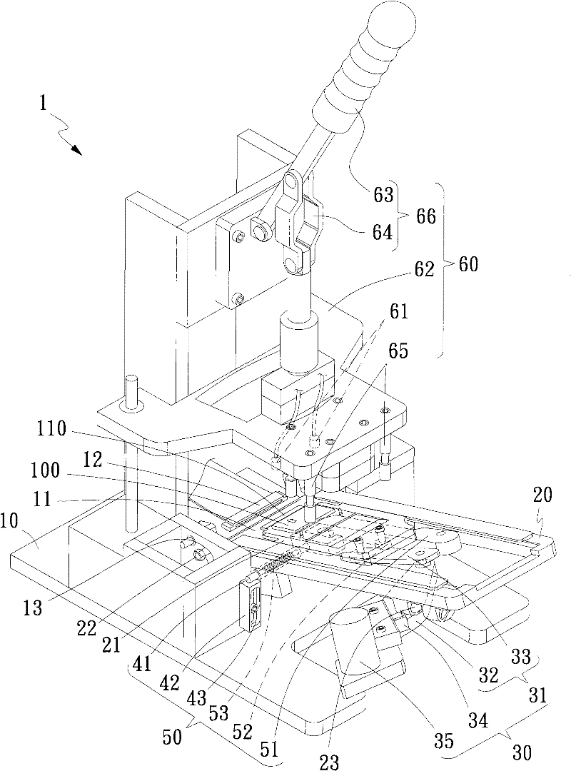
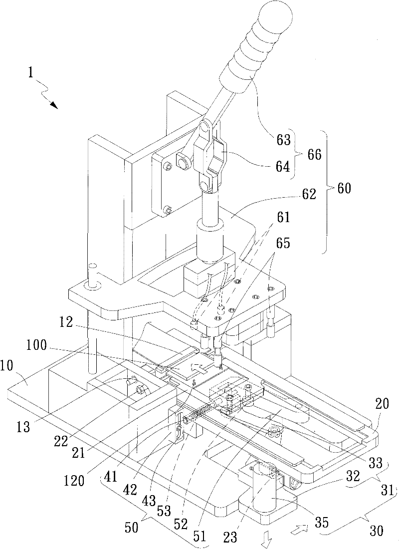
[0055] figure 1 It is a schematic diagram of a testing device 1 according to a specific embodiment of the present invention. The testing device 1 includes a base 10 , a transmission platform 20 , a driving unit 30 , an interlocking unit 50 and a testing unit 60 . The testing device 1 is used for testing a circuit board. In this specific embodiment, the circuit board 100 is a wireless network adapter card, and has a first connector 110 and two connection terminals 120, the first connector 110 can be a bus interface of PCI Express, and the connection terminals 120 can be Used to connect the receiving antenna of the product after product testing.

[0056] Referring to 1, the test device 1 includes: a base 10 with an operating area 11. In this specific embodi...


PUM


Abstract

A test device for testing a circuit board includes a base, a conveying platform, a driving unit, a connecting element, and a testing unit. The base has an operating space from above. The conveying platform is hinged to the base at a variable gradient, communicates with the operating space, and has thereon a carrier movable toward or away from the operating space as needed and configured to carry the circuit board. The driving unit is connected to the conveying platform and configured to drive the carrier to move. The connecting unit is connected to the conveying platform and the driving unit. The gradient of the conveying platform varies when the driving unit drives the carrier to move and thereby moves the connecting unit. The testing unit is movably disposed at the base and has at least one test terminal capable of approaching the operating space and testing the circuit board. Thus the test device of the invention is quick, convenient and safe and has a reduced cost.

Description

technical field [0001] The present invention relates to a testing device, in particular to a testing device for testing a circuit board. Background technique [0002] Various circuit boards, such as motherboards, display cards, network adapter cards, etc., are widely used in various electronic devices, and the yield rate of products must be controlled during production to meet quality control requirements. Therefore, product testing is usually carried out at the final stage of the production line to ensure the quality and functionality of the product. [0003] Various boards are tested in different ways depending on their functions and their inputs / outputs. Taking the product test of the wireless network card as an example, it needs to connect the wireless network card to the detection module or electronic device (such as: computer host) through the bus, and then connect the high-frequency test terminal to the connection terminal on the wireless network card, and then carry...

Claims


Application Information

Patent Timeline
Patent Type & Authority Applications(China)
IPC IPC(8): G01R31/28
CPCG01R31/2808
Inventor 赖宏明谢青峰
Owner ASKEY COMP
Why Eureka
Try Eureka