Liquid crystal display device and forming method thereof

A liquid crystal display device and liquid crystal layer technology, applied in the direction of instruments, optics, electrical components, etc., can solve the problems affecting the aperture ratio and transmittance of liquid crystal displays, hindering light from passing through liquid crystal display devices, etc., so as to improve the aperture ratio and facilitate Through, to achieve the effect of penetration

Active Publication Date: 2012-07-11
SHANGHAI TIANMA MICRO ELECTRONICS CO LTD
View PDF5 Cites 11 Cited by
  • Summary
  • Abstract
  • Description
  • Claims
  • Application Information

AI Technical Summary

Problems solved by technology

[0005] However, in the liquid crystal display device of the prior art, each pixel unit includes a plurality of spacers, and the plurality of spacers hinder a part of light from passing through the liquid crystal display device, which greatly affects the aperture ratio and transmittance of the liquid crystal display. Overrate

Method used


Image

  • Liquid crystal display device and forming method thereof
  • Liquid crystal display device and forming method thereof
  • Liquid crystal display device and forming method thereof

Examples


no. 1 example

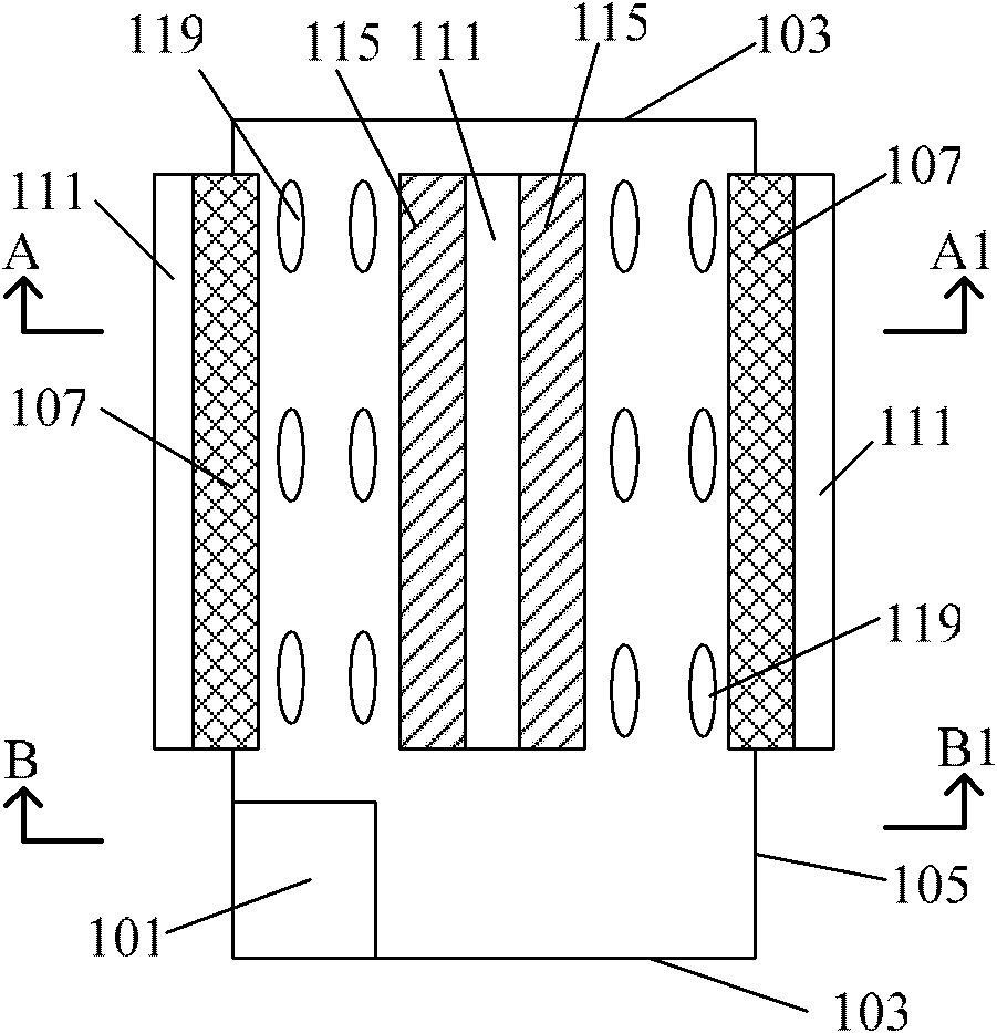
[0064] Please refer to image 3 and Figure 4 , image 3 It is a schematic structural diagram of a pixel unit of a liquid crystal display device according to the first embodiment of the present invention, Figure 4 yes image 3 A schematic cross-sectional structure diagram of the liquid crystal display device shown along line C-C1. The liquid crystal display device of the first embodiment of the present invention includes:

[0065] a first substrate 222;

[0066] a second substrate 223 opposite to the first substrate 222;

[0067] A plurality of spacers 211, 212 disposed between the first substrate 222 and the second substrate 223;

[0068] The liquid crystal layer 217 filled in the cavities formed by the plurality of spacers 211, 212, the first substrate 222 and the second substrate 223;

[0069] Each pixel unit in the liquid crystal display device according to the first embodiment of the present invention includes:

[0070] at least two spacers 211, 212;

[0071] Th...

no. 2 example

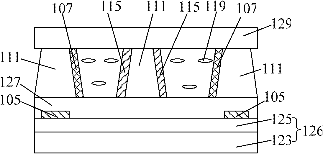
[0127] Please refer to Figure 6 and Figure 7 , Figure 6 is a schematic cross-sectional structure diagram of a liquid crystal display device according to the second embodiment of the present invention, Figure 7 yes Figure 6 A schematic cross-sectional structure diagram of the liquid crystal display device shown along line D-D1. The liquid crystal display device of the second embodiment of the present invention includes:

[0128] a first substrate 322;

[0129] a second substrate 323 disposed opposite to the first substrate 322;

[0130] A plurality of spacers 311, 312 disposed between the first substrate 322 and the second substrate 323;

[0131] a liquid crystal layer 317 filled in the cavities formed by the plurality of spacers 311, 312, the first substrate 322 and the second substrate 323;

[0132] Each pixel unit in the liquid crystal display device of the present invention comprises:

[0133] at least two spacers 311, 312;

[0134] The first substrate 322 or ...


PUM


Abstract

The invention discloses a liquid crystal display device which comprises a first substrate, a second substrate, a plurality of spacing bodies and liquid crystal layers, wherein the second substrate is opposite to the first substrate; a plurality of spacing bodies are arranged between the first substrate and the second substrate; and the liquid crystal layers are filled in cavities which are respectively formed by every two adjacent spacing bodies, the first substrate and the second substrate. The liquid crystal display device is characterized by comprising a plurality of pixel units, wherein each pixel unit comprises at least two spacing bodies, first electrodes and second electrodes; the first electrodes are positioned on the first substrate and / or the second substrate between every two adjacent spacing bodies and face to the surface of the liquid crystal layer; and the second electrodes are positioned on the opposite side walls of every two adjacent spacing bodies. According to the liquid crystal display device disclosed by the invention, transparent electrodes are adopted to replace part of spacing bodies in the prior art, and thus, the liquid crystal display device has high aperture ratio and high transmittance.

Description

technical field [0001] The invention relates to liquid crystal display technology, in particular to a liquid crystal display device in a horizontal electric field reversal mode and a forming method thereof. Background technique [0002] Generally speaking, based on the different deflection methods of liquid crystal molecules, liquid crystal displays (hereinafter referred to as LCD) can be divided into two categories: the first type is that liquid crystal molecules deflect along a plane perpendicular to the substrate, and the second type is that liquid crystal molecules deflect along a plane parallel to the substrate. plane deflection. [0003] Such as figure 1 As shown, the horizontal field switching (Horizontal Field Switching, HFS) mode liquid crystal display in the prior art is a typical second type liquid crystal display. figure 1 A pixel unit of the HFS mode liquid crystal display is shown, Figure 2a for figure 1 Sectional view along A-A1 direction, Figure 2b for...

Claims


Application Information

Patent Timeline
IPC IPC(8): G02F1/1339G02F1/1343G02F1/1362H01L21/77
Inventor 霍思涛凌志华任娇燕
Owner SHANGHAI TIANMA MICRO ELECTRONICS CO LTD
Why Eureka
Try Eureka