Eureka AIR delivers breakthrough ideas for toughest innovation challenges, trusted by R&D personnel around the world.

Stacked Chip Packaging Structure, Synchronous Rectifying Module And Converter Module

A chip packaging structure and synchronous rectification technology, applied in the direction of converting AC power input to DC power output, electric solid-state devices, semiconductor devices, etc., can solve the problems of high energy consumption, high impedance of bonding wires, and increased difficulty in making lead frame 10, etc. question

Inactive Publication Date: 2012-07-11
CHENGDU MONOLITHIC POWER SYST
View PDF7 Cites 12 Cited by
  • Summary
  • Abstract
  • Description
  • Claims
  • Application Information

AI Technical Summary

Problems solved by technology

However, the bonding wire used for electrical connection of wire-bonded chips is usually very thin and long, and the impedance of the bonding wire is relatively large, and the energy consumption is also relatively large
In addition, if the chips 11 and 12 are not thin enough, it is necessary to press down the chip attaching pad 101 of the lead frame 10 to shorten the length of the bonding wire as much as possible, but this will increase the difficulty of making the lead frame 10

Method used


Image

  • Stacked Chip Packaging Structure, Synchronous Rectifying Module And Converter Module
  • Stacked Chip Packaging Structure, Synchronous Rectifying Module And Converter Module
  • Stacked Chip Packaging Structure, Synchronous Rectifying Module And Converter Module

Examples


Embodiment Construction

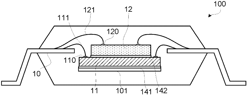
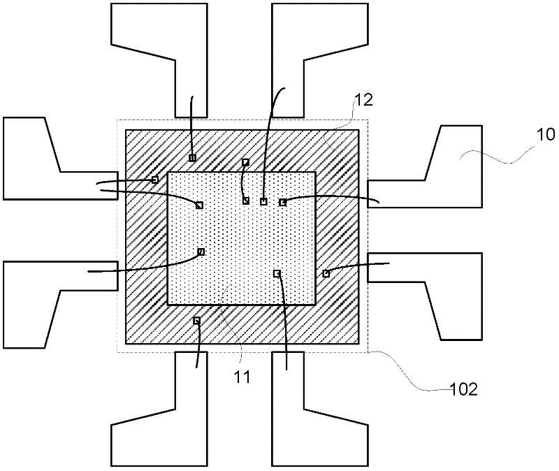
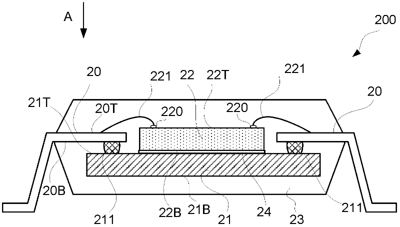
[0024] Exemplary embodiments of the present invention will be fully described below with reference to the accompanying drawings. These embodiments disclose a stacked die package structure that has both flip chip and wire bonded chips packaged therein. As used herein, "flip chip" refers to any packaged chip in which the contact areas of the chip are directly electrically coupled to the lead frame or substrate through solder bumps. The so-called "wire-bonded chip" refers to any packaged chip in which the electrical connection between the contact area and the lead frame is realized by bonding wires. The so-called "solder bump" refers to a spherical or columnar metal small piece used to directly electrically couple two contact areas, and the metal small piece is mostly filled with solder. The so-called "bonding wire" refers to a relatively small wire used to electrically couple two contact areas, and most of such wires are gold wires.

[0025] In the following detailed descripti...


PUM


Abstract

The present invention discloses a stacked chip packaging structure, a synchronous rectifying module and a converter module. The stacked chip packaging structure comprises the following components: a lead wire frame which comprises a plurality of pins; a first chip which is provided with a first surface and a second surface that opposes the first surface, wherein the first chip comprises a plurality of solder projections which are provided on the first surface, and the first chip is electrically coupled with the lead wire frame through the plurality of solder projections; and a second chip which is provided with a first surface and a second surface that opposes the first surface, wherein the second chip is electrically coupled with the lead wire frame through a plurality of bonding wires, and furthermore the second surface of the second chip adheres on the first surface of the first chip. According to the stacked chip packaging structure, the packaging dimension of the chip can be reduced and energy consumption of the chip can be reduced.

Description

technical field [0001] The present invention generally relates to a semiconductor device packaging structure, in particular to a stacked chip packaging structure, and a synchronous rectification module and a converter module using the stacked chip packaging structure. Background technique [0002] With the rapid growth of demand for miniaturization and portability of portable electronic products in the consumer electronics market in recent years, new requirements are put forward for the packaging structure of integrated circuits. Miniaturized and multi-functional electronic portable products have become the mainstream of the consumer market. The corresponding power supply system is also further developed in the direction of miniaturization, high power, multi-function and high efficiency. The multi-chip packaging structure should be developed in the direction of miniaturization and multi-function. The power discrete chip and the control chip are integrated into the same pack...

Claims


Application Information

Patent Timeline
IPC IPC(8): H01L25/00H01L23/495H02M7/00H02M1/00
CPCH01L23/49562H01L2224/32245H01L24/73H01L2224/73265H01L2224/32145H01L23/3107H01L2224/16245H01L2924/13091H01L2224/48247H01L24/32H01L23/49575H01L23/49572H01L2224/73203H01L2224/48145H01L2924/30107H01L24/16H01L2924/1425H01L24/48H01L2924/3011H01L2924/13062H01L2924/181H01L2924/14H01L2224/05554H01L2924/00014H01L2924/10162H01L2924/00H01L2924/00012H01L2224/45099H01L2224/45015H01L2924/207
Inventor 蒋航
Owner CHENGDU MONOLITHIC POWER SYST
Why Eureka
Eureka Blog
Learn More