Ultra-wideband microstrip filter

A microstrip filter and ultra-wideband technology, applied in waveguide devices, electrical components, circuits, etc., can solve the problems of not designing ultra-wideband, and achieve low return loss and good harmonic suppression

Inactive Publication Date: 2012-07-11
UNIV OF ELECTRONICS SCI & TECH OF CHINA
View PDF4 Cites 7 Cited by
  • Summary
  • Abstract
  • Description
  • Claims
  • Application Information

AI Technical Summary

Problems solved by technology

[0003] After searching relevant literature, it was found that Shau-Gang Mao et al. published a paper on Modeling of symmetric composite right/left-handed coplanar waveguides with applications to compact bandpass filters published in IEEE Transactions on Microwave Theory and Techniques in 2005. The bandpass filter in the form of coplanar waveguide has a unit structure in which a series interdigitated capacitor and a parallel meandering short-circuit stub inductor are embe...

Method used


Image

  • Ultra-wideband microstrip filter
  • Ultra-wideband microstrip filter
  • Ultra-wideband microstrip filter

Examples


Embodiment Construction

[0020] The present invention will be further described below in conjunction with the accompanying drawings and specific embodiments.

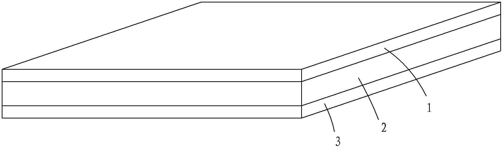
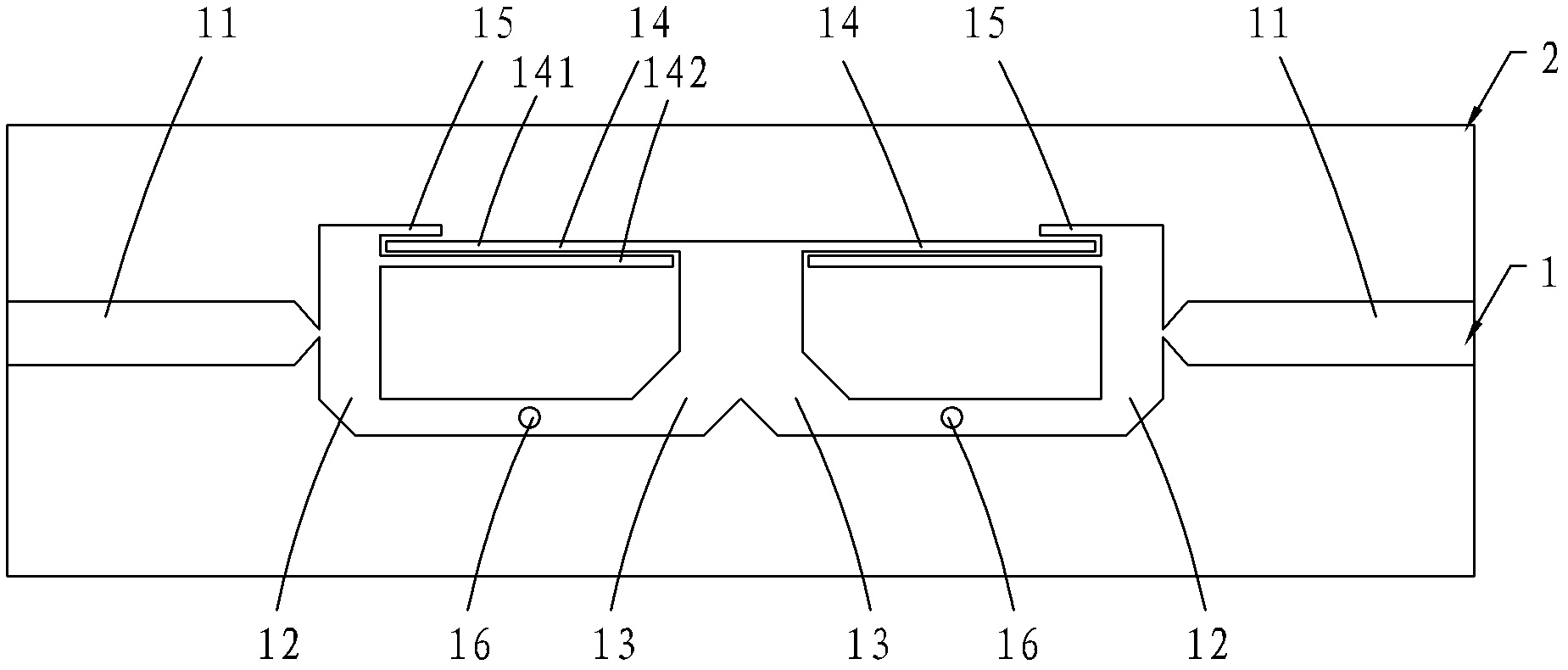
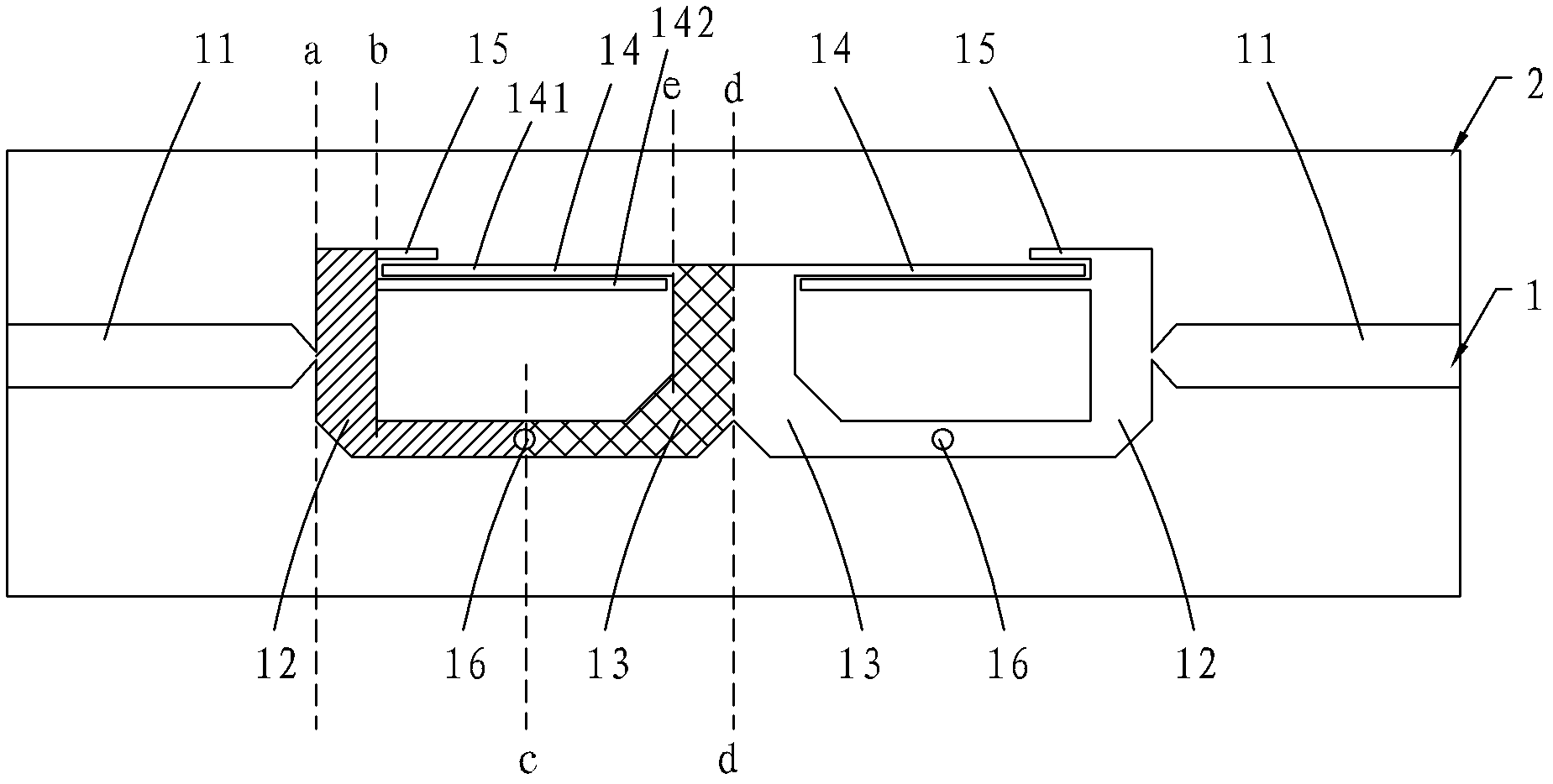
[0021] Such as figure 2 with image 3 As shown, an ultra-wideband microstrip filter includes a first metal layer 1, a dielectric layer 2, and a second metal layer 3 stacked in sequence from top to bottom, and the metal pattern of the first metal layer 1 includes left and right mirror symmetry The left metal pattern and the right metal pattern are characterized in that, the left metal pattern or the right metal pattern respectively include sequentially connected input and output ports 11, a first step impedance short-circuit stub 12, a second step The impedance short-circuit stub 13 and the cross-toe coupling line section 14, the first step impedance short-circuit stub 12, the second step impedance short-circuit stub 13 and the cross-toe coupling line section 14 form a ring structure as a resonant unit of the filter, The cross-toe coupled lin...


PUM


Abstract

The invention relates to an ultra-wideband microstrip filter which comprises a first metal layer. The metal pattern of the first metal layer comprises symmetrical left and right metal patterns, wherein the left and right metal patterns respectively comprise an input/output port, a first order stepped impedance circuit cut line, a second order stepped impedance circuit cut line and an interdigital coupling line section, and the input/output port, the first order stepped impedance circuit cut line, the second order stepped impedance circuit cut line and the interdigital coupling line section are connected in sequence. The first order stepped impedance circuit cut line, the second order stepped impedance circuit cut line and the interdigital coupling line section form a circular structure as a resonance unit of the filter. The interdigital coupling line section comprises a first sub-line section and a second sub-line section, wherein the first sub-line section and the second sub-line section are parallel to each other and are coupled with each other, the first sub-line section is connected with the tail end of the second order stepped impedance circuit cut line, and the second sub-line section is connected with the initial end of the first order stepped impedance circuit cut line. The intersection of the first and second order stepped impedance circuit cut lines is provided with a metalized through hole which penetrates through the first metal layer and a dielectric layer and forms a path together with a second metal layer.

Description

technical field [0001] The invention belongs to the technical field of ultra-wideband communication, and in particular relates to an ultra-wideband microstrip filter. Background technique [0002] In 2002, the Federal Communications Commission (FCC) of the United States opened the frequency band between 3.1 GHz and 10.6 GHz for applications in the communication field. Because of its advantages such as high transmission rate and low transmission loss, UWB communication has received extensive attention and developed rapidly. As a key device in an ultra-wideband communication system, the performance of the ultra-wideband filter determines the overall performance of the system. Generally speaking, UWB filters are required to have low passband insertion loss, good frequency selection characteristics and flat group delay in practical applications. [0003] After searching relevant literature, it was found that Shau-Gang Mao et al. published a paper on Modeling of symmetric compo...

Claims


Application Information

Patent Timeline
IPC IPC(8): H01P1/203
Inventor 肖飞张中勋
Owner UNIV OF ELECTRONICS SCI & TECH OF CHINA
Why Eureka
Try Eureka