Photoluminescence imaging systems for silicon photovoltaic cell manufacturing

A photoluminescence and imaging technology, which is applied in the direction of material excitation analysis, optical testing for flaws/defects, and material analysis through optical means, and can solve problems such as inappropriateness, slow image acquisition, and limitations

Inactive Publication Date: 2012-07-11
BT IMAGING PTY LTD
View PDF4 Cites 1 Cited by
  • Summary
  • Abstract
  • Description
  • Claims
  • Application Information

AI Technical Summary

Problems solved by technology

However, bulk silicon samples (such as ingots and bricks), as-cut silicon wafers, and precursors before passivation of photovoltaic cells are extremely poor PL radiators because their minority carrier lifetimes that determine PL intensity are limited by surface recombination. limit
Consequently, image acquisition is relatively slow for such samples, while this is generally acceptable for R&D use, or for routine inspection of bulk silicon samples, such as for identifying material before it is sawn into wafers. Areas of poorer quality. Inspection time is a critical factor if PL imaging is to be used for routine inspection of PV cells and precursors in a production environment. Current silicon wafer PV cell production lines run at 3,600 wafers per hour. , and the production rate is expected to increase
[0007] Additionally, where inspection time is not a critical factor, applicants have found that different types of silicon samples, such as as-cut wafers, surface-textured wafers, and finished photovoltaic cells, all have properties that existing PL imaging systems are not suitable for all of the above objects

Method used


Image

  • Photoluminescence imaging systems for silicon photovoltaic cell manufacturing
  • Photoluminescence imaging systems for silicon photovoltaic cell manufacturing
  • Photoluminescence imaging systems for silicon photovoltaic cell manufacturing

Examples


Embodiment Construction

[0026] In the following, preferred embodiments of the present invention are explained by way of example with reference to the corresponding drawings.

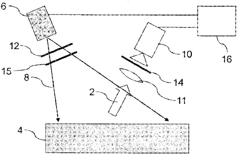
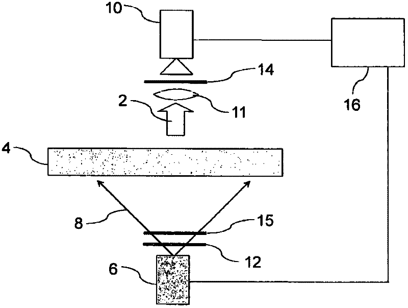
[0027] The ability of photoluminescence (PL) imaging to measure some of the desired parameters of materials is known by wafer and photovoltaic cell manufacturers and has broad and potential applications in the photovoltaic cell manufacturing industry. PL imaging is already employed in off-line test and measurement tools, for example, for surveys of poorly performing cells or for random inspection of the quality of crystals just received, and we believe in the development of different capabilities, In-line PL imaging systems with direct mechanical control or through manual operation are promising, such as wafer sorting and binning, process control feedback (e.g., to correct reject processing stages) or feed-forward (e.g., during the preparation of different grades of When feeding, adjust the processing program.)

[0028] 3(a) a...


PUM

PropertyMeasurementUnit
wavelengthaaaaaaaaaa

Abstract

A method of photoluminence (PL) imaging of a series of silicon wafers, the method including the step of: utilizing incident illumination of a wavelength greater than 808nm. The present invention further provides a method of analysing silicon semiconductor material utilising various illumination, camera and filter combinations. In some embodiments the PL response is captured by a MOSIR camera. In another embodiment a camera is used to capture the entire PL response and a long pass filter is applied to block a portion of the signal reaching the camera / detector.

Description

technical field [0001] The present invention relates to a photoluminescence imaging system for silicon photovoltaic cell production. [0002] related application [0003] This application claims priority to Australian Provisional Patent Applications Nos. 2009903823, 2009903822 and 2009903813, filed on 14 August 2009, the contents of which are hereby incorporated by reference. Background technique [0004] References in this specification to the state of the art should not be considered as widely known, or should not be considered to form part of the common general knowledge in the field. [0005] Photoluminescence (PL) imaging by the device and method disclosed in PCT Application Publication No. WO2007 / 01759A1 has been shown to be useful for imaging silicon materials and devices, especially photovoltaic cells (PV) based on silicon wafers. The value of rapid characterization; (the title of this application is Method and System for Examining Indirect Bandgap Semiconductor St...

Claims


Application Information

Patent Timeline
Patent Type & Authority Applications(China)
IPC IPC(8): G01N21/62G01N21/88
CPCG01N21/9505G01N21/6456G01N21/9501G01N21/6489
Inventor 托斯顿·特鲁普克伊恩·安德鲁·麦克斯威尔约尔根·韦伯罗伯特·安德鲁·巴多斯
Owner BT IMAGING PTY LTD
Why Eureka
Try Eureka