Low power consumption design method for SRAM (static random-access memory) type FPGA (field-programmable gate array)

A design method and low-power technology, applied in computing, special data processing applications, instruments, etc., can solve the problem of large impact on timing, affect circuit timing performance, and not further consider leakage power consumption, access logic and bypass logic and other issues to achieve the effect of reducing leakage power consumption

Active Publication Date: 2014-12-10
INST OF COMPUTING TECH CHINESE ACAD OF SCI
View PDF2 Cites 0 Cited by
  • Summary
  • Abstract
  • Description
  • Claims
  • Application Information

AI Technical Summary

Problems solved by technology

[0008] 1. The timing has a great influence
Type (1) low-power design method to configure the circuit power supply voltage and transistor threshold voltage will affect the switching characteristics of the transistor, thereby affecting the timing performance of the circuit
[0009] 2. The scope of application is limited
The low-power design method of category (1) is optimized from the perspective of FPGA chip structure, which will have an impact on the process of FPGA chip manufacturing, and is not applicable to existing FPGA chips.
[0010] 3. There is additional area overhead
The low-power design method of type (2) only considers the relationship between the output logic value of the MUX structure and the average leakage power consumption, and does not further consider the relationship between the leakage power consumption in the MUX structure and the access logic and bypass logic. Limited headroom for power optimization

Method used


Image

  • Low power consumption design method for SRAM (static random-access memory) type FPGA (field-programmable gate array)
  • Low power consumption design method for SRAM (static random-access memory) type FPGA (field-programmable gate array)
  • Low power consumption design method for SRAM (static random-access memory) type FPGA (field-programmable gate array)

Examples


Embodiment Construction

[0044] In order to make the objectives, technical solutions and advantages of the present invention clearer, the present invention will be further described in detail below with reference to the accompanying drawings. It should be understood that the specific embodiments described herein are only used to explain the present invention, but not to limit the present invention.

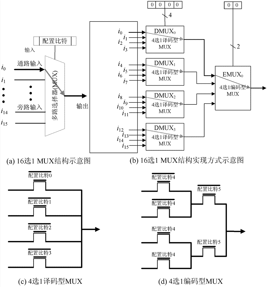
[0045] The SRAM-type FPGA is mainly composed of configurable logic modules and wiring resources. Configurable logic modules include look-up tables and flip-flops, etc., to realize the logic function of the circuit; connection resources include line segments of different lengths and switching modules connecting each line segment. The connection relationship between each line segment is realized by configuring the MUX (multiplexer) in the switching module. In the process of circuit implementation, the signal is connected from one input end of the MUX to the output end of the MUX, which is called a channel,...


PUM


Abstract

The invention provides a low power consumption design method for a SRAM (static random-access memory) type FPGA (field-programmable gate array), which includes steps: firstly, building a leakage power information graph according to structure and circuit information of the FPGA; secondly, evaluating leakage power of each MUX during wiring phase to obtain the leakage power; thirdly, importing the leakage power to wiring cost function to lower circuit leakage power. By implementing low power consumption design during the wiring phase and comprehensively considering delay consumption, congestion consumption and leakage power consumption of the circuit during the wiring process, timing performance of the circuit is hardly affected. By modifying circuit wiring manner to implement low power consumption design, the method is irrelevant with chip structure of the FPGA and suitable for current mainstream FPGA, processing of the FPGA chips is not affected and no extra area consumption is imported.

Description

technical field [0001] The present invention relates to the technical field of low power consumption design of FPGA (Field Programmable Logic Gate Array) circuit, particularly, the present invention relates to a kind of low power consumption design method of SRAM (static random memory unit) type FPGA widely used at present. Background technique [0002] For a long time, FPGA circuit has been widely concerned by circuit designers because of its short design cycle and low development cost. With the continuous improvement of chip performance, circuit design based on SRAM FPGA is widely used in communication engineering, industrial control, embedded development and other fields. However, due to the reduction of transistor feature size and the continuous reduction of threshold voltage, the leakage power consumption of SRAM FPGA increases rapidly, which has become a bottleneck restricting the further application of SRAM FPGA. The power consumption not only directly affects the pa...

Claims


Application Information

Patent Timeline
Patent Type & Authority Patents(China)
IPC IPC(8): G06F17/50
Inventor 黄柯衡胡瑜李晓维
Owner INST OF COMPUTING TECH CHINESE ACAD OF SCI
Why Eureka
Try Eureka